Members can download this article in PDF format.
The demand for mid-voltage power circuits in segments such as robotics, server farms, solar installation, RF, motor control, LiDAR, synchronous rectification, and more has put mid-range power efficiency on the map.
No longer do engineers have the luxury of design first, power efficiency second. In fact, the holy grail of semiconductor and electronic devices, in general, is to squeeze as much power as possible using the smallest-possible footprint with the least amount of energy consumption.
Power per area has been a design consideration for some time now. But recently, with predictions of global power consumption climbing to a whopping 10 TWh in the next two years and as much as 17 TWh by 2030, it’s getting a lot more attention.
To meet that lofty goal, all areas of power are being closely scrutinized. One area that can have a vast influence on power metrics is the semiconductor. New and innovative substrates and manufacturing processes are leading to measurable results in energy efficiency.
High on that list is gallium nitride (GaN). GaN technology can handle larger electric fields in a much smaller form factor than conventional silicon, allowing for a smaller component footprint.
Resources
- Mid-Voltage Applications Where GaN Will Transform Electronic Designs
- Cut Solution Size by >40% with Industry's Smallest 100V Integrated GaN Power Stages
- GaN Bidirectional Microinverter with Energy Storage Capability Reference Design
It’s estimated that 80% of the total electrical energy consumption passes through some type of power converter. Transitioning from silicon to GaN in power semiconductors presents a significant step in reducing carbon footprints and improving energy efficiency. The estimated energy savings and CO2 emission reductions from a worldwide Si-to-GaN data-center upgrade alone can reduce energy losses by 30% to 40%.
GaN: A Rising Star
Gallium nitride’s extreme hardness, high heat capacity, thermal conductivity, and wide-bandgap properties allow it to operate at higher temperatures and voltages compared to other semiconductors. GaN also has much better switching characteristics and conduction loss specifications.
Current GaN devices are basically lateral high-electron-mobility transistor (HEMT) transistors (or FETs) with exceptional conduction and switching capabilities These properties make it suitable for applications where efficient heat dissipation is essential, particularly in segments such as telecommunications, solar systems, server and data farms, and motor drives.
While GaN chips have played in the high-voltage arena (600 V and up) for some time, pressure to drive existing and emerging applications to lower operating voltages has ushered in lower-voltage GaN designs. Until recently, GaN could not be used for such designs. But the times they are a changin’.
As GaN matures, it promises much improved efficiency in power handling across the board. This will lead to smaller footprints and the ability to integrate small peripheral components (passives), shrinking the circuit footprint even further. It can reduce the energy and the physical space needed to deliver that performance of its silicon counterparts by 50% or more.
Rising to the challenge are GaN solutions developed by Texas Instruments, including the LMG2100R044—a 100-V, 4.4-mΩ, half-bridge GaN FET—and the new TIDA-010933, 1.6- kW, bidirectional microinverter.
Such components have entered the mid-voltage (100 V) application game. This opens up applications ranging from motor drives and solar inverters to electric vehicles, enterprise power delivery, smart vehicles, telecom sites, and more.
Leveraging GaN
The ability to use mid-voltage GaN devices in such applications is significant. These particular applications are some of the most power-hungry and demand five-nines reliability standards. They often have redundant power requirements, adding even more demand on energy. Using lower-voltage GaN results in significant power savings, which trickles down to other critical cost metrics such as cooling, building designs, per-watt input power costs, safety, etc.
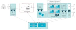
Take solar energy plants, for example. Solar energy is the fastest-growing source of renewable energy, projected to grow at an annual compound rate of nearly 12%. Imagine the cost savings and lower environmental impact realized by using devices like the LMG2100R044 and LMG3100R017 in the boost and inverter stages of the subsystems to achieve a 40% or more reduction in power and footprint (Fig. 1).
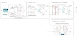
Big data is another prime target for lower-power devices. By 2030, it’s estimated that 20 million petabytes of data will be housed in data centers, globally. It’s even expected that the world will not have sufficient server farm capacity to store and manage all of this data. Therefore, smaller power supply units (PSUs), intermediate bus converters (IBCs), and backup battery systems are all prime candidates for mid-voltage, power-efficient GaN devices (Fig. 2).
In telecom infrastructure, the proliferation of radios, across all platforms and technologies, will require a much more efficient power section going forward. For example, in the 5G/6G ecosystem, many radios will not be in climate-controlled environments. In fact, most will be out in the open air.
By using GaN devices in the power-conversion stage, as well as powering inverters and RF circuits, the power-density improvement they offer means an increase in efficiency of 40% or more. It results in smaller power unit footprints and reduced operating temperatures. This broadens the location envelope and eliminates some of the cooling issues of silicon designs.
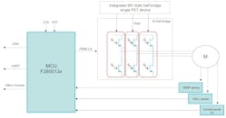
And let’s not forget motor drives (Fig. 3). With the speed that artificial intelligence and machine learning (AI/ML) is advancing, mid-range GaN devices will permeate the power sections of robots, mid-voltage electric vehicles, power tools, computers, DC-DC converters, even quantum devices.
Conclusion
Gallium-nitride power devices have shown great promise for various applications because of their high electron mobility and ability to operate at higher frequencies compared to silicon-carbide (SiC) devices. However, GaN devices still face challenges in terms of development and standardization compared to their SiC counterparts.
Companies such as TI are pushing the limits to deliver next-generation GaN devices to be prepared for the multitude of new and emerging applications and technologies that will benefit from the efficiency promised by GaN. No doubt such innovation will go a long way in taming the energy monster on the horizon and benefit the environment as well.
Resources


