This article is part of the Power Management series: How to Easily Design Power Supplies
Members can download this article in PDF format.
What you'll learn:
- What are digital power supplies?
- The effects of EMI on switch-mode power supplies.
- Designing a filter to reduce EMI.
- How Silent Switcher technology changed the game in minimizing radiated emissions.
In Part 1 of this series, we covered the LDO, switch-mode power supplies, isolation in power supplies, and the most common topologies when isolation is not required. In Part 2, we covered specialized topologies, common isolated topologies, and advanced isolated topologies. Part 3 addresses digital power supplies, EMI considerations, filtering, and silent switchers.
Digital Power Supplies
All of the power supplies discussed in this article can be implemented as analog or digital power supplies. What are digital power supplies, really? Power must always run through an analog power stage with switches, inductors, transformers, and capacitors.
The digital aspect is introduced by two digital building blocks. The first one is digital interfacing, which allows an electronic system to “talk” and “listen” to a power supply. Different parameters may be set on-the-fly to optimize the power supply for different operating conditions. Also, the power supply can communicate with a main processor and raise warning or fault flags. For example, load current, crossing a preset threshold, or excessive temperature of a power supply may easily be monitored by a system.
The second digital building block replaces an analog regulation loop with a digital loop. This can work successfully, but for most applications, the optimum is a standard analog feedback loop with some digital influence on some parameters. Such parameters include adjusting the gain of the error amplifier on-the-fly or dynamically setting the loop compensation parameters to enable a stable but fast feedback loop.
An example of a device with a purely digital control loop is the ADP1046A developed by Analog Devices. And an example of a digitally interfaced buck regulator with an analog control loop, optimized by digital influences, is the LTC3883.
EMI Considerations
Electromagnetic interference (EMI) is always a topic to pay attention to when designing switch-mode power supplies (SMPS). The reason is that SMPS switch high current flow on and off within very short periods of time. The faster the switching, the better for total system efficiency. Faster switching transitions reduce the time during which the switch is partially turned on. During this partial turn-on time, most switching losses are generated.
Figure 1 shows the waveform of the switch node of a SMPS. Let’s imagine a buck regulator. High voltage is defined by current flow through the high-side switch, and low voltage is defined by lack of current flow through the high-side switch.
In Figure 1, we can see that a SMPS doesn’t only generate noise coming from the adjusted switching frequency, but also from the switching transition speed, which is much higher in frequency. While the switching frequency usually runs between 500 kHz and 3 MHz, the switching transition time may be a few nanoseconds long. At 1-ns switching transition time, we will see 1-GHz corresponding frequency in the spectrum. At least both of those frequencies will be seen as radiated and conducted emissions. Other frequencies also may show up, coming from oscillations of the regulation loop or interactions between the power supply and filters.
There are two reasons why EMI should be reduced. The first is to protect the functionality of the electronic system that a specific power supply is powering. For example, a 16-bit ADC used in the signal path of the system should not pick up switching noise coming from the power supply. The second reason is to fulfill certain EMI regulations that are put in place by governments all over the world to protect reliable functionality of different electronic systems simultaneously.
EMI comes in two forms: radiated EMI and conducted EMI. The most effective ways of reducing radiated EMI is to optimize the PCB layout and to use technologies such as Analog Devices’ Silent Switcher technology. Certainly, it’s also effective to put the circuit into a shielded metal box. However, this may not be practical and in most cases is very costly.
Conducted EMI is typically attenuated by additional filtering. The next section will discuss such filtering to reduce conducted emissions.
Filtering
RC filters are basic low-pass filters. However, in power-supply design, every filter is nothing but an LC filter. Often, just adding some inductance in series is enough, since it will form an LC or CLC filter together with the input or output capacitors of a SMPS. Sometimes only capacitors are used as filters, but, considering the parasitic inductance on power cables or traces, together with a capacitor we form an LC filter as well. The inductor L may be an inductor with a core, or it may be a ferrite bead.
The purpose of the LC filter really is a low-pass effect, so that dc power can run through and higher-frequency disturbances are attenuated to a large degree. An LC filter has a double pole, so we get a high-frequency attenuation of 40 dB per decade. This filter has a relatively sharp drop-off.
Designing a filter isn’t rocket science. However, since parasitic components of the circuit, such as trace inductance, have an effect, modeling a filter also requires modeling the major parasitic effects. This can make simulating a filter quite time-consuming. Many designers with filter design experience know which filters have worked before, and they may iteratively optimize a certain filter for a new design.
In all filter design, one needs to not only consider the small signal behavior, such as a transfer function of a filter in a Bode plot, but also be aware of the large signal effect. In any LC filter, power runs through the inductor. If that power isn’t needed at the output anymore, due to a sudden load transient, the energy stored in the inductor needs to go somewhere. It charges up the filter’s capacitance. If the filter isn’t designed for such worst-case conditions, the stored power may cause voltage overshoots that can possibly harm circuitry.
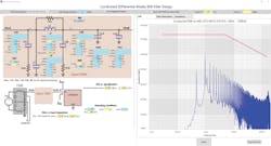
Finally, filters have a certain impedance. That impedance interacts with the impedances of the power converters attached to the filter. This interaction may lead to instabilities and oscillations. Simulation tools such as LTspice and LTpowerCAD from Analog Devices can help answer all of these questions and lead to the design of a perfect filter. Figure 2 shows the graphical user interface of the filter designer within the LTpowerCAD design environment. With this tool, filter design can be significantly simplified.
Silent Switchers
Radiated emissions are difficult to block. A special shielding with some metal material is needed, which can be very costly.
For a long time, engineers were looking for ways to reduce the radiated emissions generated by SMPS. A few years ago, a breakthrough was made with Silent Switcher technology. By reducing the parasitic inductances in the hot loops of a SMPS, and by splitting the hot loops into two and setting them up in a very symmetrical manner, radiated emissions mostly cancel each other out.
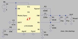
Today, many Silent Switcher devices are available, offering much lower radiated emissions than heritage products. Reducing the radiated emissions allows for switching transition speeds to increase without a serious EMI penalty. Accelerating the switching transitions reduces switching losses and thus allows for much higher switching frequencies. One example of this innovation is the LTC3310S, which can operate at 5-MHz switching frequency, enabling extremely compact designs with low-cost external components (Fig. 3).
Power Management Is a Necessity, But It Can Be Enjoyable, Too
In this three-part series, we looked at many aspects of power-supply design, including the different power-supply topologies and their advantages and disadvantages. For power-supply engineers, such information can be very basic. But for experts and non-experts alike, it’s helpful to have software tools such as LTpowerCAD and LTspice to aid in the design process. With these tools, power converters can be designed and optimized in very little time. Hopefully this series inspired you to look forward to your next power-supply design challenge.
Read more articles in the Power Management series: How to Easily Design Power Supplies


