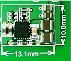
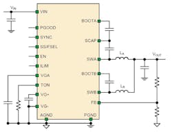
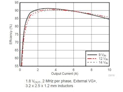
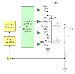
The TPS54A20 from Texas Instruments is a two-phase, synchronous series capacitor buck converter that permits small size for low-voltage applications. The IC enables efficient operation with a circuit occupying 157 mm3 that is only 1.2 mm high (Fig. 1). Small, low-profile inductors used with the TPS54A20 significantly reduce total solution area and height. Figure 2 is a simplified schematic of the TPS54A20. Figure 3 is a plot of efficiency vs. load current.
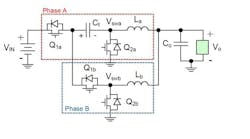
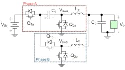
The basic series capacitor buck converter shown in Fig. 4 harnesses the hybrid switched capacitor/inductor approach. It uniquely combines a switched capacitor circuit and a multiphase buck converter in a single conversion stage. This two-phase topology adds one energy transfer capacitor (the series capacitor) that is similar to a two-phase buck converter. There are two key differences in the converter connection points that have considerable impact on converter operation and characteristics.
- The series capacitor is inserted between the high side and low side switch of phase A.
- The drain of the phase B high side switch is connected to the source of the phase A high side switch instead of the input supply.
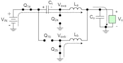
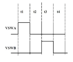
In operation, the converter has four timing intervals. During the first time interval (t1) the phase A high side switch (Q1a) turns on (Fig. 5). The phase A inductor current increases and the series capacitor is charged by the phase A inductor. The phase B low side switch (Q2b) is on and the phase B inductor current decreases. The voltage across the series capacitor is nominally half the 12V input voltage (6 V). The series capacitor value is selected so that the voltage ripple is small.
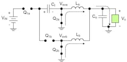
During the second and fourth time interval (t2 and t4), both low side switches (Q2a and Q2b) turn on (Fig. 6). Both switch node voltages are at ground and both inductor currents decrease. Because there is no current in the series capacitor, its voltage remains constant.
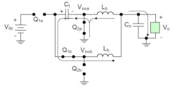
During the third time interval (t3), the phase B high side switch (Q1b) is on (Fig. 7). Because the phase A low side switch (Q2a) is also on, the negative side of the series capacitor is connected to ground. The series capacitor acts as an input capacitor to phase B and brings the phase B switch node up to approximately half the input voltage. It is discharged a small amount by the phase B inductor current, which rises during this interval and the series capacitor voltage decreases slightly.
Figure 8 shows the SWA and SWB outputs during the intervals from t1 to t4. These outputs are filtered by LA, LB, and capacitor Co to produce a DC output. Figure 9 is the output circuit of the TPS54A20.
This series capacitor buck converter differs from the conventional buck converter in several ways:
- Its duty ratio of the high side switches is doubled.
- Switching occurs with half the drain-to-source voltage experienced by switches in a buck converter.
- Its inductor current balancing is automatic.
- It exhibits decreased inductor current ripple.
All these factors are favorable for high-frequency and high-conversion ratio converters.
To improve performance during line and load transients, the TPS54A20 implements an adaptive on-time control architecture that does not require external compensation components. This architecture provides fast transient response and accurate voltage regulation at up to a 10 MHz switching frequency.
User-selectable switching frequencies are 2 MHz, 3.5 MHz, or 5 MHz per phase, which allows for efficiency and size optimization when selecting the output filter components. The on-time is adjusted based on input voltage and oscillator frequency. An internal phase lock loop (PLL) ensures fixed-frequency operation of the converter over the entire load range and adapts the on-time accordingly.
The TPS54A20 contains an internal oscillator for steady-state, fixed-frequency operation that is set through the SS/FSEL pin. The controller operates at double the per-phase switching frequency (that is, 4 MHz, 7 MHz, or 10 MHz) and the oscillator is set accordingly. An external synchronization clock can also be provided via the SYNC pin.
This IC starts up safely into loads with pre-biased outputs (non-zero volts at startup). It implements an internal under voltage lockout (UVLO) feature on the VIN pin with a nominal starting voltage of 7.65 V. The total operating current for the TPS54A20 is approximately 6 mA when not switching and under no load. When disabled by pulling the EN pin low, supply current is typically less than 50 µA.
A power good comparator (PGOOD) monitors the output voltage via the FB pin. The PGOOD pin is an open-drain MOSFET that is pulled low when the FB pin voltage is less than 95% or greater than 105% of the reference voltage (VREF). The PGOOD pin floats (de-asserted) when the FB pin voltage is between 95% to 105% of VREF. The PGOOD pin is held low during startup or when a fault occurs.
The EN pin provides power-supply sequencing capability during power up. Soft start times for each frequency can be selected through the SS/FSEL pin. Soft start helps to minimize inrush currents. You can set the device current limit via the ILIM pin that has two user-selectable current limits.
The output voltage is set by connecting a resistor divider network from the output voltage to the FB pin of the device and to AGND. It is recommended that the lower divider resistor maintain a range between 1 kΩ and 10kΩ.
Selecting the value of the upper resistor can change the output voltage between 0.508 V and 2 V. The minimum output setpoint voltage cannot be less than the 0.508 V reference voltage. The maximum output voltage can be limited by minimum input voltage. The recommended minimum input voltage should be at least five times the output voltage due to the nature of the series capacitor buck converter.
Series Capacitor Monitoring
The series capacitor voltage is preconditioned and monitored during operation. This capacitor is located between the source of the high-side MOSFET and the drain of the low-side MOSFET in Phase A. After the input voltage is above UVLO and the EN pin is high, the series capacitor is pre-charged. A 10 mA current source charges the series capacitor up to half the input voltage. When the series capacitor pre-charge is complete, the soft start sequence begins. The delay due series capacitor pre-charge is:
Where:
CT = Series capacitance in µF
IPC = Pre-charge current in mA
VIN = Input voltage
The voltage monitor continuously tracks the status of the series capacitor to ensure its voltage, measured differentially between the SCAP pin and the SWA pin, stays within pre-defined thresholds. These two thresholds are relative to VIN with respect to PGND and set at 35% and 65% of VIN.
The 35% of VIN threshold detects a series capacitor undervoltage fault. If the 35% threshold is breached, the converter shuts down, and PGOOD is pulled low. After the fault hiccup time completes, the converter starts up in the normal manner. The start-up sequence begins with pre-charging the series capacitor to half the input voltage and is followed by the soft start.
The 65% of VIN threshold indicates a series capacitor overvoltage fault has occurred. If the 65% threshold is breached, a fault is triggered, the converter shuts down, PGOOD is pulled low, and an internal bleed resistor is connected to the SCAP to reduce the series capacitor voltage. After the fault hiccup time is complete, the converter will start up in the normal manner.
A major function of the series capacitor is energy transfer, which is a different role from input and output capacitors where decoupling is their primary function. Here, the design objective is to ensure the series capacitor voltage ripple does not exceed 5% to 10% of the nominal voltage under the worst case conditions. Selection of the series capacitance, CT, depends on the amount of allowable ripple:
Where:
= Allowable voltage ripple percentage
fsw = Switching frequency
VIN(MIN) = Minimum input voltage
For example, if the voltage ripple target is 5%, the value for is 0.05. The largest voltage ripple occurs at full load current (highest IOUT), highest duty ratio (lowest input voltage/highest output voltage), and lowest frequency. For this design example, the value for was selected to
be 0.08. The resulting series capacitance calculated is 1.85 μF. Therefore, select a 10 V, X7R, 2.2 μF ceramic capacitor.
Another consideration is the capacitor’s RMS current rating, which impacts the temperature rise of the capacitor. Check the capacitor datasheet for temperature rise information. If the temperature rise is too large for a single capacitor, multiple capacitors may be placed in parallel to share the RMS current.
Multilayer ceramic capacitors (MLCC) are well suited for operation as the series capacitor. The equivalent series resistance (ESR) is relatively low (for example, 5 mΩ to 10 mΩ), which helps to reduce power loss and self heating. The equivalent series inductance (ESL) is fairly low, which results in a high self-resonant frequency (SRF). A key item that should be considered is the effect of capacitance variation. The effective capacitance decreases with DC bias, which means that the capacitor should be selected based on its capacitance with the nominal voltage of VIN/2 applied. Temperature variation also reduces effective capacitance. So use X7R capacitors with up to 125°C operating temperature range. If capacitors are not properly selected, cracking or other failure modes may result.
Series Capacitor Buck Converter Advantages
This topology overcomes two major challenges to high-frequency operation of buck converters: excessive switching loss and narrow high side switch pulse width. For example:
- Operation at MHz switching frequencies can cause a large switching loss that increases proportionally with switching frequency. High voltage conversion ratio (e.g. >5:1) and high current (e.g. >10 A) can also add to switching loss.
- Narrow pulse widths can be difficult to generate effectively without other time delays interfering with maintaining sufficient room for control. Many converters using peak current mode control find it difficult to generate short on-times because they must blank the initial portion of the high side on-time. Plus, narrow pulse width can be a limiting factor in high voltage conversion ratio applications, like a 5 MHz buck converter with a 10:1 voltage conversion ratio may have a high side switch nominal on-time of 20ns.This short on-time is not achievable in many converters.
