A medical system employs a 1-kW, four-phase, interleaved single-stage PFC circuit that provides a regulated 150-V dc from a single-phase 115-V ac, 60-Hz power source. This regulator serves as the intermediate bus, which then drives a 1-kW resonant driver to create a high output voltage.
The four-phase interleaved single-stage PFC is patterned after a design that appeared in the March 2006 issue of Power Electronics Technology. In that design, four 250-W, 100-kHz frequency synchronized modules, phased at 90-degree increments, were utilized to minimize component stress and cost while offering design scalability and modularity.
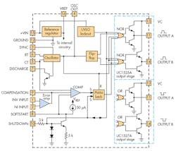
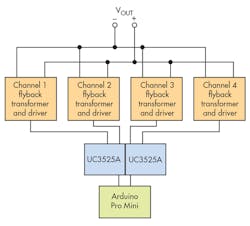
This four-channel circuit uses two Texas Instruments UC3525A PWM ICs (Fig. 1). The UC3525A is a pulse-width-modulator (PWM) IC that boosts performance and lowers the external parts count when used in a switch-mode power supply. The on-chip +5.1-V reference is trimmed to 1% and the input common-mode range of the error amplifier includes the reference voltage, eliminating external resistors.
A sync input to the PWM’s oscillator allows multiple units to be slaved or a single unit to be synchronized to an external system clock. A single resistor between the CT and the discharge terminals provides a wide range of dead-time adjustment. These devices also feature built-in soft-start, requiring only an external timing capacitor.
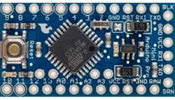
After considering many options, an Arduino Pro Mini microcontroller was selected to provide the two phase-shifted synchronizing signals to the PWM controllers. The Arduino Pro Mini microcontroller board (Fig. 2) employs Atmel’s ATmega328, a low-power CMOS 8-bit microcontroller based on the AVR enhanced RISC architecture.
Arduino Pro Mini is intended for semi-permanent installation in objects. The board comes without pre-mounted headers, allowing the use of various connector types or direct soldering of wires. The pin layout is compatible with the Arduino Mini. This approach costs slightly more than a discrete logic version. There are two versions of the Pro Mini—one runs at 3.3 V and 8 MHz; the other at 5 V and 16 MHz. The card was designed and is manufactured by SparkFun Electronics.
The Arduino microcontroller offers ceramic resonator accuracy, and supports software modification if additional modules are incorporated in future applications. The Arduino can also add a slight amount of frequency dithering to reduce EMI. Such flexibility justifies the increased cost.
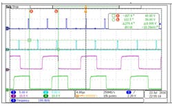
Timing pulses in each channel are synchronized so that they are 90 degrees apart. Synchronization was derived from custom code that generates the output of the Arduino to be fed into the sync pins of the PWM. The sync pulses look like those in Figure 3.
Figure 4 shows the four-flyback circuit. VOUT has four flyback channels wired in parallel. The flybacks all have lossless snubbers on the primaries that consist of a small inductor and capacitor. Each channel has 120-Hz rectified dc from the line (caution: not isolated). The controller comprises the two UC3525A voltage-mode PWM ICs.
The UC3525A has two 180-degree phased outputs. In the PFC circuit, two PWM controllers are frequency-synchronized and 90-degree phase-shifted, which equally spaces each of the four power modules by 90 degrees. The PWM outputs are further buffered using MIC4420 MOSFET drivers that subsequently drive the flyback MOSFETS.
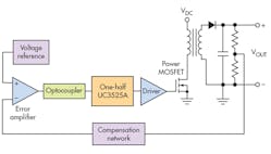
Figure 5 shows one channel of the flyback circuit consisting of the UC3525 PWM controller, driver, power MOSFET, and transformer.
By recirculating power-transformer leakage inductance using resonant lossless snubbers on each of the flyback MOSFETs, the efficiency is kept as high as possible, which is a challenge for a discontinuous flyback. An optocoupler isolates the output-connected feedback amplifier from the input-referenced PWM controllers. The controller is primary-referenced and the output is secondary-referenced.
Because the control loop is a critical and demanding part of the design, an injection resistor and probe test points for gain/phase measurements were added to optimize measurability. The injection point is buffered by the feedback amplifier and connected ahead of the optocoupler current-limiting resistor.
The Bode 100 and the Injector are used to measure and optimize the control loop. The control-loop bandwidth has to be well below 60 Hz or PFC will be lost, and it must have good stability or significant overshoot could occur during turn on (also leading to poor transient response).
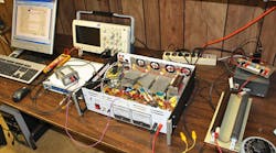
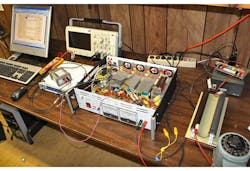
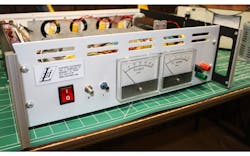
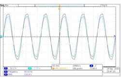
The setup for the prototype system is shown in Figure 6. On the right are load resistors and a Variac for adjusting the ac input voltage. Figure 7 depicts the complete supply and Figure 8 compares the input voltage with the power-factor-corrected output.
