This article is in the TechXchange: Why Low Iq is the Smart Thing to Do.
Members can download this article in PDF format.
What you'll learn:
- Rise in applications demanding low-quiescent-current electronics.
- A nanowatt boost power converter for medical implants.
- Devices used in bioelectronic neurostimulation.
- What is an adaptive pulse-skip modulation buck power converter?
During my electronic circuit design career from 1972 to 2013, I had many applications for low-power, low-quiescent-current designs. These kinds of designs will greatly challenge designers to optimize a solution that meets the overall required system performance, in addition to keeping the quiescent current at or below the power performance goal.
Silicon Devices Then and Now
Back in 1947, low-power silicon electronic devices began to appear on the scene, when vacuum power tubes, with their excessive power needs, began to be replaced by the industry-changing, orders-of-magnitude smaller in size and power draw, point-contact transistor. Bell Labs’ John Bardeen, Walter Brattain, and William Shockley rocked the electronics world.
Fast-forwarding to 2023, the relentless demand for low-power electronics is driven by three distinct applications:
- Portable electronic products such as tiny hearing aids, life-saving cardiac pacemaker implants, multifunction electronic wristwatches, small calculators (fitting on your wrist), personal digital assistants, and so much more.
- The ever-increasing packaging density of functional devices in integrated circuits (ICs) for enhanced performance along with tight restrictions on power dissipation.
- The continued reduction of power in desktop and laptop systems, where a competitive lifecycle cost-performance ratio demands low power, leading to ongoing reduction of power-supply and cooling costs.
Another low-power trend is shrinking IC temperature, leading to higher reliability. This also enables the use of low-cost plastic packages.
Low-Iq Power-Management Units for Implants
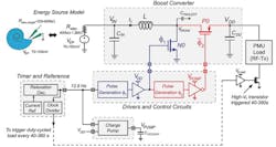
Figure 1 shows a nanowatt boost power converter,1 pulse-generation circuitry ɸ1 and ɸ2 for drivers, and control circuitry for an autonomous wireless sensor. This power-management unit (PMU) sustains itself via harvesting energy from the endocochlear potential (EP), which is a 70- to 100-mV electrochemical bio-potential. In addition, two electrodes connected to the PMU are inserted within a mammalian inner ear that will tap the EP.
The total extractable power from the EP is limited to just 1.1 to 6.25 nW. This is where the nanowatt boost converter comes into play, increasing the input voltage from 30 to 55 mV to 0.8 to 1.1 V. Now this voltage is usable by CMOS circuitry within the sensor. The picowatt charge pump (Fig. 1, again) minimizes the leakage in the boost converter.
Ultra-low-power control circuitry, which is made up of digital usage of input-impedance adjustment circuits and zero-current-switching circuits in addition to timer and reference circuits (Fig. 1, again), will maintain the quiescent power of the PMU down to 544 pW.
The nanowatt boost power converter can reach a peak power-conversion efficiency of 56%. The PMU is able to sustain itself, plus a duty-cycled ultra-low-power load, while extracting power from the EP of a live guinea pig. The PMU circuits were fabricated on a 0.18-µm CMOS process.
Miniaturized Electronics for Neurostimulation
Research in bioelectronic medicine sometimes employs scaled-down electronic systems for nerve stimulation. Long lifetimes, high precision, and very small size is a prerequisite in this medical electronics field.
Generating precise stimulation pulse trains usually necessitates the use of a microcontroller with a software-defined, pulse-width-modulated (PWM) output. In this case, an accurate pulse train can be generated without using a microcontroller. This method will enable size reduction along with power savings.
Many small animal stimulators are able to attain submillimeter sizes via ultrasonic or inductive carriers for the stimulation signal as a mechanism for power delivery. This approach leads to two limitations:
- The subject must be close to the coils or transducers at all times. This limits range of motion.
- Low-complexity systems might not be capable of verifying the state of the device operation.
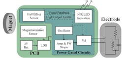
Figure 2 shows the stimulator proposed in this method.2
The amazing thing about a device like that in Figure 2 is not only is the device designed for ease of manufacture, as well as being constructed with only low-cost, commercially available off-the-shelf (COTS) components, but it also has a target manufacturing time of one month.
The quiescent current is down to 1.4 μA and the active current is at 160 μA with default stimulation parameters (250-μA amplitude, 32-Hz frequency, 100-μs pulse width). As a result, this device can be powered by just a single 3-V lithium battery cell for as long as 147 days with two hours of stimulation each day.
An Adaptive Pulse-Skip Modulation Buck Converter
The IoT continues to develop and grow at a rapid pace. This growth has led to the accelerated deployment of wireless sensor nodes (WSNs) in such applications as smart grid systems, home automation, and wearables.
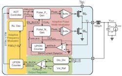
These types of applications are best supported by an adaptive pulse-skip modulation (APSM) buck power converter, which features low quiescent current along with a wide dynamic range capability (Fig. 3).3
The features of low Iq, suppressed output ripple, and enhanced transient response time are possible due to an adaptive on-time (AOT) technique. Dynamic range is extended via the suppressed output ripple.
The proposed buck converter is capable of reaching 96% peak efficiency with a dynamic range of 106 and an 8-nA quiescent current. These features make the APSM buck converter ideal for IoT systems-on-chips (SoCs).
Ultra-Low-Iq Capacitor-Less LDO
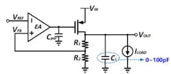
This section discusses a capacitor-less low-dropout (CL-LDO) regulator with an ultra-low quiescent current and fast transient response (Fig. 4).4
Adaptive stage and dual power transistors are used to simplify the LDO’s topology at light load. This method will enable ultra-low Iq and can ensure LDO performance under heavy loads.
To further enhance the transient response, a co-enhanced transient circuit was introduced by adding an extra switching current, which improves the slew rate without consuming very much quiescent current. Simulation results show that the design can achieve a 12-nA quiescent current and less than 500-ns settling time. The proposed LDO is well-suited for high-energy-efficiency IoT applications with mode switching.
Summary
There are no “tricks” to designing a system for low quiescent current. Designers need to minimize quiescent current by understanding the tradeoff between managing extended battery life and achieving a high-performance design.
Designers seeking high efficiency, along with a no- or light-load condition, must employ a power solution that can tightly regulate their system output with the goal of maintaining an ultra-low supply current. This article brings some creative design ideas and methods to keep quiescent current at a minimum in most any type of electronic design.
Read more articles in the TechXchange: Why Low Iq is the Smart Thing to Do.
References
1. “A 1.1 nW Energy-Harvesting System with 544 pW Quiescent Power for Next-Generation Implants,” IEEE Journal of Solid-State Circuits, Vol. 49, No. 12, December 2014.
2. “A low-power implantable neurostimulator for small rodents with functional validation,” Institute for Bioelectronic Medicine, Feinstein Institutes for Medical Research Northwell Health, Manhasset, NY, USA, 2019.
3. “A 96% Peak Efficiency Adaptively Controlled PSM Buck Converter with Low-Quiescent Current and Wide Dynamic Range for IoT Applications,” IEEE Solid-State Circuits Letters, Vol. 5, 2022.
4. “A 12 nA Ultra-Low Quiescent Current Capacitor-Less LDO with 350 ns Fast Transient Response,” 2022 IEEE 4th International Conference on Circuits and Systems.


