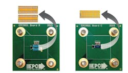
We can evaluate the thermal performance of the eGaN monolithic half-bridge IC. The first eGaN monolithic half-bridge IC5 is the same size as single discrete eGaN FET and has similar package thermal impedances from junction-to-board and junction-to-case. For half-bridge layouts, thermal evaluation boards were built to the same specifications as discussed in the previous section and shown in Fig. 25. It is anticipated that the eGaN monolithic half-bridge IC, due to its factor of two reduction of chip size, should be at a thermal disadvantage.
25. Thermal evaluation boards implementation for eGaN FET based half bridges with discrete transistors (left) and an eGaN monolithic half-bridge IC (right).
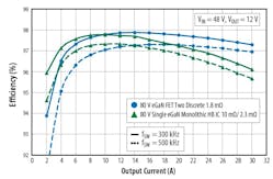
The total system efficiency comparisons of the eGaN FET based 48 VIN to 12 VOUT buck converters operated at switching frequencies of 300 kHz and 500 kHz are shown in Fig. 26. This includes losses of the entire system, including the inductor (4.7 μH Coilcraft SER2915L), capacitors, and PCB losses. The eGaN monolithic half-bridge IC (80 V EPC21054) based design offers higher light-load efficiency than the design with two discrete eGaN FETs (80 V EPC20214) as a result of the smaller chip size, reducing the switching related losses. At full load, the two discrete eGaN FET based design, which have a lower on-resistance, demonstrates higher efficiency by providing lower conduction losses. At 500 kHz, the eGaN monolithic half-bridge IC based design widens its advantage at lighter loads compared to the larger discrete solution.
26. Experimental efficiency comparison between monolithic and discrete eGaN FET based buck converters.
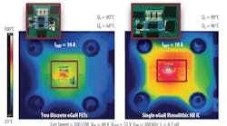
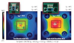
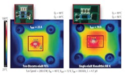
In Fig. 27, the thermal performance of the discrete eGaN FET and eGaN monolithic half-bridge IC based designs are compared. At 18 A with an airflow of 200 LFM, the eGaN monolithic half-bridge IC based design approaches 100°C. The discrete eGaN FET based design has lower device temperatures of 19°C and 28°C, respectively on the top device (Q1) and low-side device (Q2). The thermal performance advantage of the discrete based eGaN FET design is expected here, since the discrete solution has lower power loss in this evaluation case and larger chip area to dissipate heat. The eGaN monolithic half-bridge IC, which has the highest power density solution evaluated in this chapter, exhibits comparable thermal performance to the best Si MOSFET based design, which is shown in Fig. 14.
27. Experimental thermal comparison between discrete eGaN FET (left) and eGaN monolithic half-bridge IC (right) based buck converters.
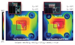
For the same maximum temperature, the discrete eGaN FET based design can be run to 22 A, where the maximum device temperature matches that of the eGaN monolithic half-bridge IC on the top device (Q1), while the low-side (Q2) eGaN FET runs 12°C cooler as shown in Fig. 27. From the thermal images in Figs. 27 and 28, two major thermal advantages of the monolithic integration can be seen. The first advantage is that the monolithic-based solution efficiently distributes heat between the two devices, which are located on a single chip with lower thermal impedance between the devices. This ensures good thermal balancing between the two devices and maximize the overall thermal capability of the system.
For the discrete eGaN FET based solution shown on the left in Figs. 27 and 28, the device Q1 has a much higher temperature than the device Q2 and is the thermally limiting device of the system. For the eGaN monolithic half-bridge IC based design, there is a very small 3°C temperature difference across the eGaN monolithic half-bridge IC. For the monolithic design, the higher loss device, Q1, can use the larger active area (and lower thermal resistance path) of the device Q2 to spread the heat and achieve much better overall thermal performance.
The second thermal advantage of the eGaN monolithic half-bridge IC is the ability of the monolithic solution to reduce the board-to-ambient resistance of the system (RθBA). For the discrete eGaN FET based design shown on the left in Fig. 25, the top device (Q1) is located above the bottom device (Q2) and below the input capacitors (CIN). This limits the access Q1 has to the large copper planes used to reduce the board-to-ambient thermal impedance.
Another thermal challenge for Q1 is that in a half-bridge configuration it has no connection to ground. In the majority of PCB designs, the ground plane occupies the largest portion of the overall board space and is therefore a very good thermal path for the system. By monolithically integrating the two devices into a single chip, the top device (Q1), will have good thermal paths to the large ground plane, reducing the board-to-ambient impedance of the system and maximizing thermal performance.
28. Experimental thermal comparison between discrete eGaN FET (left) and eGaN monolithic half-bridge IC (right) based buck converters, with same maximum device temperature.
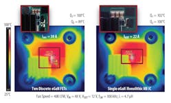
In Figs. 29 and 30, the thermal performance of the discrete eGaN FET and eGaN monolithic half-bridge IC based designs are compared with heat sinks added to the designs. The discrete eGaN FET based design, with a larger chip area, and therefore lower junction-to-case impedance and case-to-ambient impedance, shows a much larger relative advantage when adding a heat sink. For the eGaN monolithic half-bridge IC based design, the achievable output power can be increased by 22% by adding a heat sink.
29. Experimental thermal comparison between discrete eGaN FET (left) and eGaN monolithic half-bridge IC (right) based buck converters with heat sinking.
30. Experimental thermal comparison between discrete eGaN FET (left) and eGaN monolithic half-bridge IC (right) based buck converters with heat sinking, with same maximum device temperature.
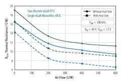
The equivalent junction-to-ambient thermal impedances, as shown in Fig. 31, were calculated for the discrete and eGaN monolithic half-bridge IC based designs. In the case without a heat sink and 400 LFM airflow, the eGaN monolithic half-bridge IC based design has around 14% higher thermal impedance than the discrete eGaN FET based design, despite having only half the chip area. In the case with a heat sink and 400 LFM airflow, the eGaN monolithic half-bridge IC based design has around 30% higher thermal impedance than the discrete eGaN FET based design.
31. Comparison of junction-to-ambient system thermal impedance vs. airflow for discrete eGaN FET and eGaN monolithic half-bridge IC based buck converters.
Thermal Figure of Merit
Various electrical figures of merit (FOM) were compared for eGaN FETs and Si MOSFETs with each figure of merit being a simple tool to quickly compare different technologies. Also, each figure of merit focuses on different applications. While these FOMs gave valuable insight into the electrical performance achievable with a given device technology, they gave no insight into thermal performance, which is also critical in power converter design. We will introduce a thermal figure of merit for designers to be used as a tool to quickly compare the thermal efficiency of given devices packaging technology. This thermal FOM will be compared for the eGaN FET and Si MOSFET packaging technologies used.
As shown in Figs. 5 and 6, the thermal capability of a package can be determined by two parameters, RθJC and RθJB, the junction-to-board and junction-to-case thermal impedances. These thermal impedances scale with the size of a given package technology, with a larger device having lower thermal impedance. The thermal efficiency of a package is related to its ability to dissipate heat based on a given chip area.
To compare the thermal efficiency of a given packaging technology a thermal figure of merit is proposed:
Where ADEVICE is the size of the packaged device. For design cases where heat can be removed from both the PCB and backside of the device (RθBA ≈ RθCA):
For cases where the dominant heat removal path is through the PCB (RθBA << RθCA):
And for cases where the dominant heat removal path is the backside of the device (RθBA >> RθCA):
Assuming the device can be effectively cooled through the PCB and the backside of the device, the thermal FOM can be given by:
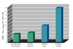
Comparing the thermal FOM for eGaN FETs chip-scale packages and the state-of-the-art Si MOSFET packages used for comparison in this chapter, the thermal efficiency advantages of the chip-scale package can be seen, as shown in Fig. 32—with the eGaN FET packaging having almost a 2× reduction in FOMTH, as compared to the best Si MOSFET package. The chip-scale package offers true double-sided cooling and therefore the best overall thermal performance based on the size of the chip.
32. Thermal figure of merit comparison of eGaN FET chip-scale packages and state-of-the-art Si MOSFET packages at a frequency of 300 kHz.
References
- D. Reusch and J. Strydom, “Understanding the Effect of PCB Layout on Circuit Performance in a High-frequency Gallium Nitride Based Point-of-Load Converter,” Applied Power Electronics Conference and Exposition (APEC), pp. 649-655, 2013.
- D. Reusch, D. Gilham, Y. Su, and F. C. Lee, “Gallium Nitride Based 3D Integrated Non-Isolated Point-of-Load Module,” Applied Power Electronics Conference and Exposition (APEC), pp. 38-45, 2012.
- Efficient Power Conversion Corporation, “EPC demonstration boards.”
- Efficient Power Conversion Corporation, “EPC eGaN FETs.”
- D. Reusch, J. Strydom, and A. Lidow, “Monolithic Integration of GaN Transistors for Higher Efficiency and Power Density in DC-DC Converters,” International Exhibition and Conference for Power Electronics, Intelligent Motion, Renewable Energy and Energy Management (PCIM Europe), pp. 986-993, 2015.
- A. Lidow, J. Strydom, M. de Rooij, D. Reusch, GaN Transistors for Efficient Power Conversion, Second Edition, Chichester, United Kingdom, Wiley, 2014.
- Ralph Locher, “Introduction to Power MOSFETs and their Applications,” Fairchild Semiconductor Application Note 558, 1998.
- “Thermal Design Basics,” Analog devices MT-093 Tutorial, 2009.
- “DirectFET® Technology Thermal Model and Rating Calculator,” International Rectifier Application Note AN-1059, 2010.
