This articles is part of the Power Management Series in the Power Management section of our Series Library.
Download this article as a .PDF eBook.
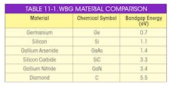
Wide bandgap (WBG) semiconductor materials allow smaller, faster, more reliable power electronic components and with higher efficiency than their silicon-based counterparts. These capabilities make it possible to reduce weight, volume, and life-cycle costs in a wide range of power applications. Harnessing these capabilities can lead to dramatic energy savings in industrial processing and consumer appliances, accelerate widespread use of electric vehicles and fuel cells, and help integrate renewable energy onto the electric grid.
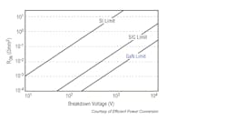
WBG semiconductors permit devices to operate at much higher temperatures, voltages, and frequencies—making the power electronic modules using these materials significantly more powerful and energy-efficient than those made from conventional semiconductor materials. Figure 11-1 compares the breakdown voltages of silicon and WBG semiconductors SiC and GaN.
11-1. Comparison of breakdown voltage for Si, SiC, and GaN.
WBG semiconductors are expected to pave the way for exciting innovations in power electronics, solid-state lighting, and other diverse applications across multiple industrial and clean energy devices with vastly superior performance compared to current technology. Projected WBG benefits are:
- Elimination of up to 90% of the power losses that currently occur during ac-to-dc and dc-to-ac power conversion.
- Operation up to 10 times higher than Si-based devices, which will enhance high-power performance.
- Operation up to higher maximum temperature of Si-based devices, which will provide better overall system reliability.
- Enabling of smaller and lighter systems with reduced lifecycle energy use, along with opportunities for new applications.
- Operation at higher frequencies than Si-based devices, making possible more compact, less costly product designs.
As manufacturing capabilities improve and market applications expand, costs are expected to decrease, making WBG-based devices competitive with less expensive Si-based devices. Several manufacturing challenges must be addressed to make WBG materials more cost effective, including:
- Cost of producing larger-diameter wafers needs to be reduced.
- Novel device designs that effectively exploit the properties of WBG materials are needed to achieve the voltage and current ratings required in certain applications.
- Alternative packaging materials or designs are also needed to withstand the high temperatures in WBG devices.
- Existing systems may have to be redesigned to integrate the WBG devices in ways that deliver their unique capabilities.
SiC
Using SiC (silicon carbide) can reduce on-resistance to two orders of magnitude in compared with existing Si devices. Use of SiC devices can reduce power loss extensively, when applied to power conversion systems. These SiC devices such as power MOSFET or IGBT are used in combination with rectifier devices such as Schottky barrier diode (SBD). SiC-SBD has been introduced. Within the last few years, SiC power MOSFETs have been manufactured after being able to produce usable SiC material.
GaN
Silicon power MOSFETs have not been able to keep pace with evolutionary changes in the power electronics systems industry. The power electronics industry reached the theoretical limit of silicon MOSFETs and now must go to another semiconductor material whose performance matches today’s newer systems. The new material is gallium nitride (GaN), a high electron mobility (HEMT) semiconductor, which is poised to usher in new power devices that are superior to the present state of the art. Although GaN is young in its life cycle, it will certainly see significant improvements in the years to come.
Gallium nitride (GaN) is grown on top of a silicon substrate. The end result is a fundamentally simple, elegant, cost-effective solution for power switching. This device behaves similarly to Silicon MOSFETs with some exceptions.
GaN transistors behave in a similar manner to silicon power MOSFETs. A positive bias on the gate relative to the source causes the device to turn on. When the bias is removed from the gate, the electrons under it are dispersed into the GaN, recreating the depletion region, and once it the capability to block voltage. Among GaN’s features:
1. GaN offers superior performance compared with both silicon and silicon carbide.
2. Device-grade gallium nitride can be grown on top of silicon wafers.
3. GaN-on-silicon offers the advantage of self-isolation and therefore efficient monolithic power integrated circuits can be fabricated economically.
4. Enhancement-mode (normally off) and depletion mode (normally on) GaN devices are available.
SiC Power MOSFET
Cree is the first to come up with a viable MOSFET. The ability to make these parts rests on the gate structure, which requires a physics and chemistry solution. The company still has some “tweaking” to do with the process, but it appears to be well ahead of the other companies that have ventured into this technology.
The commercial production of 1200 V SiC power MOSFETs is now feasible because of recent advances in substrate quality, improvements in epitaxy, optimized device design, advances made in increasing channel mobility with nitridation annealing, and optimization of device fabrication processes. SiC is a better power semiconductor than silicon (Si) because SiC has a much higher electric field breakdown capability (almost 10x), higher thermal conductivity, and higher temperature operation capability (wide electronic band gap).
SiC excels over Si as a semiconductor material in 600V and higher-rated breakdown voltage devices. SiC Schottky diodes at 600V and 1200V ratings are commercially available today and are already accepted as the best solution for efficiency improvement in boost-converter topologies as well as in solar inverters by substituting them for the previously used Si PiN free-wheeling diodes that have significant switching losses
The SiC MOSFET being discussed here is a 1200V, 20A device from Cree that has a 100mΩ RDS(on) at a +15V gate-source voltage. Besides the inherent reduction in on-resistance, SiC also offers a substantially reduced on-resistance variation over operating temperature. From 25°C to 150°C, SiC variations are in the range of 20% versus 200% to 300% for Si. The SiC MOSFET die is capable of operation at junction temperatures greater than 200°C, but for this particular example it is limited by its TO-247 plastic package to 150°C.
The technology also benefits from inherently low gate charge, which allows designers to use high switching frequencies and thereby specify smaller passive components such as inductors and capacitors.
GaN Power Transistors
Performance of silicon-based MOSFETs is reaching its upper performance limit. One company developing a higher performance alternative is Efficient Power Conversion (EPC). EPC produces gallium nitride (GaN) on silicon wafers using standard MOS processing equipment. EPC produces gallium nitride on silicon wafers using standard MOS processing equipment. GaN’s exceptionally high electron mobility and low temperature coefficient allows very low RDS(ON), while its lateral device structure and majority carrier diode provide exceptionally low QG (total gate charge) and zero QRR (source-drain recovery charge). As a result, GaN devices can handle tasks benefitted by very high switching speeds.
Initially, GaN-on-silicon transistors were depletion mode types. That is, they operated like a normally on power switch that required a negative voltage to turn them off. The ideal mode for designers is an enhancement mode transistor that is normally non-conducting and requires a positive voltage to turn it on, like the present silicon-only N-channel MOSFETs. EPC produces an enhancement mode GaN transistor using a proprietary process with a GaN-on-silicon structure. In operation, a positive gate voltage turns the enhancement mode GaN transistor on.
An advantage of the GaN transistor is that its blocking voltage rating depends on the distance between the drain and gate; the longer the distance, the higher the voltage rating. Another GaN advantage is its very low on-resistance.
GaN transistors borrowed the same nomenclature as their silicon brethren: gate, drain, and source, as shown Fig. 11-2. In addition, on-resistance and breakdown voltage of a GaN device have a similar meaning as their silicon counterparts. On-resistance (RDS(ON)) versus gate-source voltage curves are similar to silicon MOSFETs. The temperature coefficient of GaN FETs on-resistance is similar to the silicon MOSFET as it is positive, but the magnitude is somewhat less.
11-2. Enhancement mode GaN has a circuit schematic similar to silicon MOSFETs with gate (G), drain (D), and source (S).
GaN has a higher critical electric field strength than silicon. Its higher electron mobility enables a GaN device to have a smaller size for a given on-resistance and breakdown voltage than a silicon semiconductor. Compared to silicon devices, this also allows devices to be physically smaller and their electrical terminals closer together for a given breakdown voltage requirement.
The two types are the depletion mode and enhancement mode. The depletion mode transistor is normally on and is turned off with a negative voltage relative to the drain and source electrodes. In contrast, the enhancement mode transistor is normally off and is turned on by positive voltage applied to the gate. Depletion mode transistors are inconvenient because at start-up of a power converter, a negative bias must first be applied to the power devices or a short circuit will result. Enhancement mode devices do not have this problem: with zero bias on the gate, an enhancement mode device is off and will not conduct current.
The threshold of enhancement mode GaN FETs is lower than that of silicon MOSFETs. This is made possible by the almost flat relationship between threshold and temperature along with the very low gate-to-drain capacitance (CGD). The device starts to conduct significant current at 1.6V, so care must be taken to ensure a low impedance path from gate-to-source when the device needs to be held off during high speed switching in a rectifier function.
The threshold of depletion mode GaN HEMTs ranges from -5 V to -20 V.
Besides its low RDS(ON), the lateral structure of the enhanced GaN FET also makes it a very low-capacitance device. It can switch hundreds of volts in nanoseconds, giving it multi-megahertz capability. With a lateral structure, CGD comes only from a small corner of the gate and is much lower than the same capacitance in a vertical MOSFET.
Gate-to-source capacitance (CGS) consists of the junction from the gate in channel, and the capacitance of the dielectric between the gate and the field plate. CGS is large compared with CGD, giving GaN FETs good dv/dt immunity, but still small compared with silicon MOSFETs. The drain-to-source capacitance (CDS) is also small, being limited to the capacitance across the dielectric from the field plate to the drain. Capacitance versus voltage curves for GaN FETs are similar to those for silicon, except that for a similar resistance, its capacitance is significantly lower.
The GaN transistor structure is a purely lateral device, without the parasitic bipolar junction common to silcon MOSFETs. Therefore, the enhancement GaN reverse bias or “diode” operation has a different mechanism, but a similar function. With zero bias gate-to-source there is an absence of electrons under the gate region. As the drain voltage decreases, a positive bias on the gate is created relative to the drift region, injecting electrons under the gate. Thus, there are no minority carriers involved in conduction, and therefore no reverse recovery losses.
Although QRR is zero, output capacitance (COSS) has to be charged and discharged with every switching cycle. For devices of similar RDS(ON), enhancement GaN FETs have significantly lower COSS than silicon MOSFETs. It takes a bias on the gate greater than the threshold voltage to turn on the enhancement FET in the reverse direction; the forward voltage of the “diode” is higher than silicon transistors.
In the cascode configuration for depletion mode devices, the low-voltage silicon MOSFET has very low QRR due to its body diode, which is orders of magnitude lower than a high-voltage silicon device with similar ratings to the high-voltage HEMT.
The three most important GaN FET parameters are:
- Maximum allowable gate voltage
- Gate threshold voltage
- Body diode voltage drop
The maximum allowable gate-source voltage for an enhanced GaN FET of 6V is low compared with traditional silicon. The gate voltage is also low compared to most power MOSFETs, but does not suffer from as strong a negative temperature coefficient. And, the body diode forward drop can be a volt higher than comparable silicon MOSFETs.
Because the total Miller charge (QGD) is much lower for an eGaN FET than for a similar on-resistance power MOSFET, it is possible to turn on the device much faster. Too high a dv/dt can reduce efficiency by creating shoot-through during the “hard” switching transition. It would therefore be an advantage to adjust the gate drive pull-up resistance to minimize transition time without inducing other unwanted loss mechanisms. This also allows adjustment of the switch node voltage overshoot and ringing for improved EMI. For eGaN FETs, where the threshold voltage is low, the simplest general solution is to split the gate pull-up and pull-down connections in the driver and allow the insertion of a discrete resistor as needed.
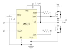
11-3. EPC GaN transistors employ the Texas Instruments’ LM5113 half-bridge gate driver IC.
The LM5113, from Texas Instruments, is an example of an eGaN FET optimized half-bridge driver that implements bootstrap regulation (Fig. 11-3). Integrated in the undervoltage lockout is an overvoltage clamp that limits bootstrap voltage to 5.2 V ensuring sufficient reliable operation under all circuit conditions. In addition to the clamp, there are separate source and sink pins, >50 V/ns dv/dt capability, matched propagation time, 0.5 Ω pull down, and separate high-side and low-side inputs to unlock the efficiencies the eGaN FETs enable.
PE29100
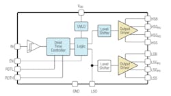
The PE29100 from Peregrine Semiconductor, now pSemi, (Fig. 11-4) is an integrated high-speed driver intended to control the gates of external power devices, such as enhancement mode gallium nitride (e.g. eGaN) transistors. The outputs of the PE29100 are capable of providing switching transition speeds in the sub-nanosecond range for hard switching applications up to 33 MHz. The PE29100 is available in a flip chip package.
11-4. PE29100 functional diagram.
The PE29100 is manufactured on Peregrine’s UltraCMOS process, a patented variation of silicon-on-insulator (SOI) technology on a sapphire substrate, offering the performance of GaAs with the economy and integration of conventional CMOS.
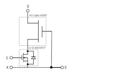
To allow normally off operation of a depletion mode GaN HEMT, it is often packaged in cascode with a low-voltage silicon MOSFET to allow normally off operation. The cascode configuration provides the ruggedness of a silicon gate, coupled with the improved voltage blocking characteristics of a high-voltage GaN HEMT. Figure 11-5 shows the cascode configuration with a depletion mode HEMT employed by Transphorm. There are no special requirements for the gate driver since the gate is connected to a standard silicon gate rated at ±20 V with threshold around 2 V.
11-5. Transphorm employs a cascode circuit to drive the GaN device. Drain, gate, and source are similar to a silicon MOSFET’s D, G, and S, and K is the Kelvin contact for the gate return.
The layout is most critical regardless if the device is e-mode, d-mode, or cascode configuration. All of these devices switch extremely fast and therefore the parasitic inductance of the layout must be as small as possible; in the range of 0.4 nH to 2.0 nH is desirable.
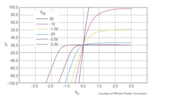
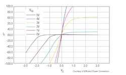
There are two types of GaN transistors, enhancement mode and depletion mode. Enhancement mode is normally off and is turned on by a positive pulse. Depletion mode is normally on and is turned off by a negative pulse. Output characteristics of a depletion mode GaN transistor are in Fig. 11-6. Figure 11-7 shows the output characteristics of an enhancement mode GaN transistor.
11-6. Output characteristics of a depletion mode GaN transistor.
11-8. LMG5200 half-bridge with GaN output transistors and internal gate drivers.
Propagation delays between the high-side gate driver and low-side gate driver are matched to allow very tight control of dead time. Controlling the dead time is critical in GaN-based applications to maintain high efficiency. HI and LI can be independently controlled to minimize the third quadrant conduction of the low-side FET for hard switched buck converters. A very small propagation mismatch between the HI and LI to the drivers for both the falling and rising thresholds ensures dead times of <10 ns. Co-packaging the GaN FET half-bridge with the driver ensures minimized common source inductance.
This minimized inductance has a significant performance impact on hard-switched topologies.
The built-in bootstrap circuit with clamp prevents the high-side gate drive from exceeding the GaN FETs maximum gate-to-source voltage (VGS) without any additional external circuitry. The built-in driver has an undervoltage lockout (UVLO) on the VDD and bootstrap (HB-HS) rails. When the voltage is below the UVLO threshold voltage, the device ignores both the HI and LI signals to prevent the GaN FETs from being partially turned on. Below UVLO, if there is sufficient voltage (VCC > 2.5 V), the driver actively pulls the high-side and low-side gate driver output low. The UVLO threshold hysteresis of 200 mV prevents chattering and unwanted turn-on due to voltage spikes. Use an external VCC bypass capacitor with a value of 0.1 μF or higher. A size of 0402 is recommended to minimize trace length to the pin. You should place the bypass and bootstrap capacitors as close to the device as possible to minimize parasitic inductance.
All-SiC 300A
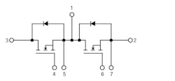
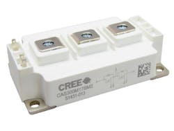
Cree’s, now Wolfspeed's, all-SiC 300A, 1.2kV half-bridge module circuit (Fig. 11-9) is packaged in industry-standard 62mm housing (Fig. 11-10). The module reduces energy loss due to switching by more than five times compared to the equivalent silicon solution. This efficiency enables an all-SiC high power converter rated up to the megawatt level.
11-9. Configuration of the Cree half-bridge.
The all-SiC 62mm half-bridge module allows designers to reduce the amount of magnetic and cooling elements, delivering double the power density and a lower system cost while also reducing end user cost of ownership. Offering a simplified two-level topology that is feasible at higher frequencies, the new module can also eliminate the need to invest in multi-level silicon-based solutions.
This Cree SiC power module is available with multiple gate driver options and is pin-compatible to standard 62mm half-bridge modules, including IGBT modules rated at 450A or more. This allows designers to quickly and easily evaluate the module’s unparalleled capabilities.
The all-SiC 300A, 1.2kV half-bridge module is available as part number CAS300M12BM2. Companion gate drivers are also available.
11-10. The all-SiC 300A, 1.2kV half-bridge module is packaged in industry-standard 62mm housing.
A newer module design also configured as in Fig. 11-9 is said to be the industry’s most optimized to achieve the unique benefits of SiC technology—with a 66% reduction in module inductance to 5.5nH, compared to competitive power products at 15nH. This reduction in module inductance enables faster switching speeds, higher frequency operation, and ultra-low losses.
Available as part number CAS325M12HM2, the high-performance power module is configured in a half-bridge topology comprised of seven 1.2kV 25mΩ C2M SiC MOSFETs and six 1.2kV 50A Z-Rec Schottky diodes. The companion gate driver (CGD15HB62LP) is specifically designed for integration with the module to fit within the 62mm mounting footprint. An engineering evaluation kit that includes both the module and the gate driver is also available so design engineers can quickly and easily test the performance of the new device in their systems.
Read more articles from the Power Management Series in the Power Management section of our Series Library.

