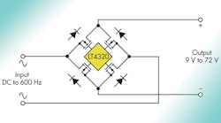
Full-wave diode bridges are found in many electronic systems (Fig. 1). At typical AC power line voltages, the drop across the diodes has little impact on the rectified output voltage and diode power dissipation. However, diodes in low voltage, high power rectification applications dissipate significant power and the inherent diode drops take a significant bite out of the operating voltage. For example, power dissipation of the diode bridge in Fig. 1 is:
P = 2 × 0.6 V × IL (1)
Where:
IL = Line current in amperes
P = Power dissipation in watts
0.6 V = Typical voltage drop for one conducting rectifier diode
At IL = 1 A dissipation is 1.2 W, at 10 A it’s 1 2 W, and at 100 A it’s 120 W. High diode power dissipation can require heat sinking to maintain diode temperature within reliability limits. Heat sinks add assembly costs, occupy board area, add weight, and obstruct cooling airflow. Plus, diode heat can affect neighboring circuits, which may require a fan that adds noise and decreases power efficiency and reliability. Therefore, heat dissipated by a high power diode bridge affects power conversion cost and efficiency.
Related Articles
- Are Schottky and Conventional Diodes Obsolete?
- Analyzing Full-Wave Rectifiers with Capacitor Filters
- Selecting Filter Capacitors forThree Phase Bridge Rectifiers
- 2011 Rectifier/Diode Review
The impact of the 1.2 V drop from two conducting diodes depends on the input voltage. For example, the drop is only 0.7% of a 170 V (peak voltage for 120 VAC) input. However, as a percentage of the input voltage it is 10% of a 12 V input and 13.3% of 9 V inputs.
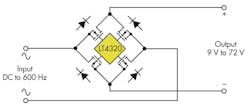
One solution to cutting the diode power loss is to use the LT4320 (Fig. 2) that controls a bridge of four N-channel MOSFETs. The LT4320 operates with inputs of 9 V to 72 VDC or 12 V/ 24 AC. Compared with the high power, low voltage four diode bridge, the part :
• Reduces power dissipation
• Increases available voltage
• Reduces power supply size
• Improves power efficiency
• Eliminates the need for bulky heat sinks
• Provides extra margin by saving two diode voltage drops
Compared with the traditional diode bridge alternative, the MOSFET bridge enables a space- and power-efficient rectifier design.
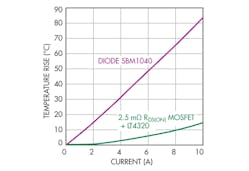
The LT4320 controller smoothly turns on the appropriate two MOSFETs, while keeping the other two off to prevent reverse currents. The choice of MOSFETs offers design flexibility for power levels from one to thousands of watts. Fig. 3 compares board temperature rise for both the diode and MOSFET bridges on similar PCBs.
An integrated charge-pump facilitates the all N-channel MOSFET design, simplifying the Bill of Materials (BOM) compared with a circuit using a mix of N- and P- channel MOSFETs. N-channel MOSFETs are smaller, more economical and offer a wider performance selection than their P-channel cousins. The LT4320’s integrated charge pump provides at least 425 µA of pull-up current to turn on the top-side N-channel MOSFET gate. The strong pull-up current enables rectification for high frequency inputs and high power applications employing large gate charge MOSFETs.
There are two MOSFET rectifier bridge controller versions; the LT4320 specified for DC to 60Hz rectification, and the LT4320-1 for DC to 600Hz. Specified over the −40 oC to 85 oC industrial temperature range, the LT4320 is offered in a compact 8-pin 3mm x 3mm DFN package, and a 12-lead MSOP package with enhanced high-voltage pin spacing. An extremely simple and space-saving solution, it offers both leaded and leadless package choices, depending on the end application and board assembly capability.
MOSFET Selection
A good starting point is to reduce the MOSFET bridge power dissipation to 1/10 that of an equivalent diode rectifier bridge, which yields a 70 mV drop. (Note that it is possible to design a lower drop for even lower power dissipation.) For a 24 W, 12 VDC application, IAVG = 2 A, so select RDS(ON) to be:
Where:
IAVG = Average output load current in amperes
In the AC power input calculation, 3 × IAVG assumes the duration of current conduction occupies 1/3 of the AC period. For 24 VAC operation, IAVG = 1 A, so select RDS(ON) to be:
Select the maximum allowable drain-source voltage, VDSS, so it is higher than the maximum input voltage. Ensure that the MOSFET can handle a continuous current of 3 × IAVG to cover the expected peak currents during AC rectification. That is, select ID ≥ 3 A. A 24 VAC waveform can reach 34V peak, so select a MOSFET with VDSS >>34 V. A good choice of VDSS is 60 V in a 24 VAC application.
Other Considerations
Choose the lowest available total gate charge, QG, and correspondingly the lowest CISS, COSS, and CRSS. Choosing a lower gate capacitance while meeting RDS(ON) speeds up the response time for full enhancement, regulation, turn-off, and input shorting events. VGS(th) (gate threshold) must be a minimum of 2 V or higher. A gate threshold voltage lower than 2 V is not recommended because it requires too much time to discharge the gate below the threshold and halt current conduction during a hot plug or input short event.
Place a 1 μF ceramic and a 10 μF minimum electrolytic capacitor across the OUTP and OUTN pins with the 1 μF ceramic placed as close to the LT4320 as possible.
Downstream power needs and voltage ripple tolerance determine the required additional capacitance between OUTP and OUTN. A common value for CLOAD is hundreds to thousands of microfarads. A good starting point is selecting CLOAD so that:
Where:
VRIPPLE = Maximum tolerable output ripple voltage
Freq = Frequency of the input AC source
For example, in a 60 Hz, 24 VAC application where the load current is 1 A and the tolerable ripple is 15 V, choose
Select CLOAD so that the rectified output voltage, OUTP-OUTN, is within the LT4320/LT4320-1 specified OUTP voltage range.
Applications
The LT4320 applications include up to 50 VAC or 72 VDC rectification, PoE PDs with auxiliary 24 VAC/12 V-DC inputs such as security cameras and wireless access points (WAPs), and 400 Hz airborne power distribution.


