This article is part of the TechXchange: Gallium Nitride (GaN).
Why Gallium Nitride?
The power semiconductor evolution started with germanium and selenium devices that succumbed to silicon types around the 1950s. Broader silicon usage stemmed from its improved physical properties combined with a large investment in manufacturing infrastructure and engineering. However, silicon power MOSFETs have not kept pace with evolutionary changes in the power electronics systems industry. The power electronics industry reached the theoretical limit of silicon MOSFETs and now must go to another semiconductor material whose perfromance matches today’s newer systems. The new material is gallium nitride (GaN) a high electron mobility (HEMT) semiconductor, whaich is poised to usher in new power devices that are superior to the present state of the art. Although GaN is young in its life cycle, it will certainly see significant improvements in the years to come.
What nomenclature do GaN devices employ?
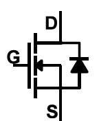
GaN transistors borrowed the same nomenclature as their silicon brethren: gate, drain and source, as shown Fig. 1. In addition, on-resistance and breakdown voltage of a GaN device have a similar meaning as their silicon counterparts. On-resistance (RDS(ON)) vs. gate-source voltage curves are similar to silicon MOSFETs. The temperature coefficient of GaN FETs on-resistance is similar o the silicon MOSFET as it is positive, but the magnitude is significantly less.What is the primary advantage of GaN over silicon power transistors?
GaN has a higher critical electric field strength than silicon. Its higher electron mobility enables a GaN device to have a smaller size for a given on-resistance and breakdown voltage than a silicon semiconductor. Compared to silicon devices, this also allows devices to be physically smaller and their electrical terminals closer together for a given breakdown voltage requirement.
What are the two types of GaN power semiconductors?
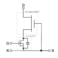
The two types are the depletion mode and enhancement mode. The depletion mode transistor is normally on and is turned off with a negative voltage relative to the drain and source electrodes. In contrast, the enhancement mode transistor is normally off and is turned on by positive voltage applied to the gate. Depletion mode transistors are inconvenient because at start-up of a power converter, a negative bias must first be applied to the power devices or a short circuit will result. Enhancement mode devices do not have this problem: with zero bias on the gate, an enhancement mode device is off and will not conduct current.To allow normally off operation of a depletion mode GaN HEMT, it is often packaged in cascode with a low voltage silicon MOSFET to allow normally off operation. The cascode configuration provides the ruggedness of a silicon gate, coupled with the improved voltage blocking characteristics of a high voltage GaN HEMT (Fig. 2).
How does a GaN’s Gate threshold voltage function?
The threshold of enhancement mode GaN FETs is lower than that of silicon MOSFETs. This is made possible by the almost flat relationship between threshold and temperature along with the very low gate-to-drain capacitance (CGD). The device starts to conduct significant current at 1.6 V, so care must be taken to ensure a low impedance path from gate-to-source when the device needs to be held off during high speed switching in a rectifier function.
The threshold of depletion mode GaN HEMTs ranges from -5 V to -20 V.
What are the important capacitances in a GaN FET?
Besides its low RDS(ON), the lateral structure of the enhanced GaN FET also makes it a very low capacitance device. It can switch hundreds of volts in nanoseconds, giving it multi-megahertz capability. With a lateral structure, CGD comes only from a small corner of the gate and is much lower than the same capacitance in a vertical MOSFET.Gate-to-source capacitance (CGS) consists of the junction from the gate in channel, and the capacitance of the dielectric between the gate and the field plate. CGS is large compared with CGD, giving GaN FETs good dv/dt immunity, but still small compared with silicon MOSFETs. The drain-to-source capacitance (CDS) is also small, being limited to the capacitance across the dielectric from the field plate to the drain. Capacitance vs. voltage curves for GaN FETs are similar to those for silicon, except that fir a similar resistance, its capacitance is significantly lower.
Does the GaN FET have a body diode?
The GaN transistor structure is a purely lateral device, without the parasitic bipolar junction common to silcon MOSFETs. Therefore, the enhancement GaN reverse bias or “diode” operation has a different mechanism, but a similar function. With zero bias gate-to-source there is an absence of electrons under the gate region. As the drain voltage decreases, a positive bias on the gate is created relative to the drift region, injecting electrons under the gate. Thus, there are no minority carriers involved in conduction, and thefore no reverse recovery losses. Although QRR is zero, output capacitance (COSS) has to be charged and discharged with every switching cycle. For devices of similar RDS(ON), enhancement GaN FETs have significantly lower COSS than silicon MOSFETs. It takes a bias on the gate greater than the threshold voltage to turn on the enhancement FET in th reverse direction, the forward voltage of the “diode” is higher than silicon transistors.In the cascode configuration for depletion mode devices, the low voltage silicon MOSFET has very low QRR due to its body diode, which is orders of magnitude lower than a high voltage silicon device with similar ratings to the high voltage HEMT.
What are the important enhanced GaN FET driving Requirements?
The three most important parameters are:
- Maximum allowable gate voltage
- Gate threshold voltage
- Body diode voltage drop
The maximum allowable gate-source voltage for an enhanced GaN FET of 6 V is low compared with traditional silicon. The gate voltage is also low compared to most power MOSFETs, but does not suffer from as strong a negative temperature coefficient. And, the body diode forward drop can be a volt higher than comparable silicon MOSFETs.
Because the total Miller charge (QGD) is much lower for an eGaN FET than for a similar on-resistance power MOSFET, it is possible to turn on the device much faster. Too high a dv/dt can reduce efficiency by creating shoot-through during the ‘hard’ switching transition. It would therefore be an advantage to adjust the gate drive pull-up resistance to minimize transition time without inducing other unwanted loss mechanisms. This also allows adjustment of the switch node voltage overshoot and ringing for improved EMI. For eGaN FETs, where the threshold voltage is low, the simplest general solution is to split the gate pull-up and pull-down connections in the driver and allow the insertion of a discrete resistor as needed.
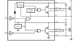
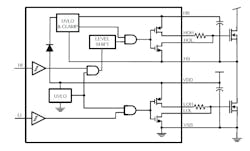
The LM5113, from Texas Instruments, is an example of an eGaN FET optimized half bridge driver that implements bootstrap regulation. Integrated in the undervoltage lockout is an overvoltage clamp that limits bootstrap voltage to 5.2 V ensuring sufficient reliable operation under all circuit conditions. In addition to the clamp, there are separate source and sink pins, >50 V/ns dv/dt capability, matched propagation time, 0.5 Ω pull down, and separate high side and low side inputs to unlock the efficiencies the eGaN FETs enable.
Fig. 3 shows the cascode configuration with a depletion mode HEMT, there are no special requirements for the gate driver since the gate is connected to a standard silicon gate rated at ±20V with threshold around 2V.
For the cascode configuration with a depletion mode HEMT, there are no special requirements for the gate driver since the gate is connected to a standard silicon gate rated at +/- 20 volts with threshold around 2 volts.
What is most critical about using GaN devices?
The layout is most critical regardless if the device is e-mode, d-mode or cascode configuration. All of these devices switch extremely fast and therefore the parasitic inductance of the layout must be as small as possible, in the range of 0.4 nH to 2.0 nH is desirable.
What are the projections for future GaN products?
Figure 4 is EPC’s projection of the future of GaN devices. When originally introduced in 2010, devices were rated at 40 to 200 V and 500 Mhz switching speed. Recent introductions by EPC raised the speed up to 3 GHz for devices rated at 40 V, 65 V and 100 V and on-resistance ranging from 125 mΩ to 530 mΩ. The company also expects GaN transistors to eventually operate at 600 V and it expects more functions per chip.


