Increasingly, many industrial PCs (IPCs), USB power delivery (PD), and automotive digital video recorders (DVRs) require wide VIN DC/DC converters to cope with a wide range of battery voltage transients. The power demand for such applications also keeps increasing. Wide input-range, along with high power requirements, makes power supply design extremely challenging.
A four-switch buck-boost converter is very suitable for such wide VIN applications since it can maintain output voltage regulation when the battery voltage fluctuates above or below the desired output voltage level. Additionally, the four-switch buck-boost converter features synchronous rectification and, therefore, has the potential to achieve high efficiency in high-power applications. This article explains how to address wide VIN and high-power challenges using four-switch buck-boost converters. Furthermore, practical measures to extend power capability, improve efficiency, and enhance thermal performance are discussed.
Four-Switch Buck-Boost Converter
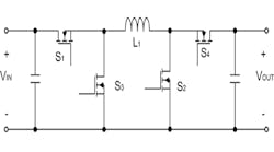
A four-switch buck-boost converter (Fig. 1) employs single-inductor architecture to realize either step-down or step-up dc/dc conversion as needed. Synchronous rectification is expected to reduce conduction loss and improve efficiency particularly in high current applications.
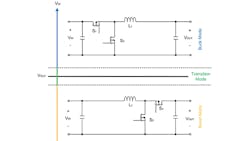
A state-of-the-art four-switch buck-boost controller, such as TI’s LM5175, controls the four switches and operates the four-switch buck-boost converter in three different operation modes. As illustrated in Fig. 2, it operates in buck mode when VIN is higher than VOUT, boost mode when VIN is lower than VOUT, and transition mode when VIN and VOUT are close to each other. Seamless transfer from one mode to another can be achieved using proper control. In such buck or boost operation modes, the four-switch buck-boost converter is nearly as efficient as a basic buck or boost converter.
Practical Measures to Extend Power Capability
High efficiency and good thermal performance are two of the top priorities for power supply design, which are extremely critical in high-power, high-current applications. For instance, a buck-boost converter is required to deliver 200W of power from a battery in some IPC applications. The battery voltage ranges from 9V to 36V, which suggests up to 22.2A DC current, even if the buck-boost converter’s efficiency is 100 percent. The actual worst case current is even larger when taking the efficiency factor into account. Such high power and current will generate excessive heat dissipation, if the design is not done properly. Besides the power board itself, the excessive heat might also heat up the surrounding components, such as the hard-disk due to the compact design, which is unacceptable.
It is worth pointing out again that four-switch buck-boost converters benefiting from synchronous rectification and buck or boost mode control have the potential to achieve high efficiency. Some further practical measures can be taken to maximize efficiency and minimize temperature rise. As such, the high-power requirement can be handled without adding heat-sink.
Paralleling Two MOSFETs for Each Switch
Generally, a MOSFET used in a synchronous four-switch buck-boost converter has lower conduction loss than a Schottky diode. Another difference between a MOSFET and diode is the positive temperature coefficient of the MOSFET’s on-resistance. As the temperature rises, the on-resistance of MOSFET increases, and so does the forward voltage drop. This characteristic makes current flow equally through multiple MOSFETs when they are connected in parallel and prevents thermal runaway. In contrast, a Schottky diode has a negative temperature coefficient. Hence, a MOSFET is more suitable for parallel operation in high-current applications.
In terms of conduction loss reduction, positioning MOSFETs in parallel is very effective. The conduction loss of the MOSFET (PCON) in watts is:
Where:
IRMS = Root mean square (RMS) current flowing through the MOSFET
RDS(ON) is the MOSFET’s on-state resistance
Unlike the Schottky diode, a MOSFET has linear I-V characteristic. Reducing the MOSFET current to half its original value also reduces the MOSFET conduction loss to half its original value. When two MOSFETs are connected in parallel, the total conduction loss PCON(TOTAL) becomes:
The conduction loss reduction improves the overall efficiency. Also, the conduction loss in every single MOSFET when two of them are connected in parallel now is only quarter of that when only one MOSFET is used. As such, the temperature rise and thermal performance is significantly improved.
Adding Schottky Diodes with Rectifier MOSFETs
In a synchronous four-switch buck-boost converter, MOSFETs (S3 and S4 in Fig. 1) rather than diodes are used as rectifier, which reduces conduction loss. However, the body diode of S3 conducts during dead-time in buck mode, while the body diode of S4 conducts during dead-time (tDEAD) in boost mode. The dead-time loss can be calculated as:
Where:
VF = Forward voltage drop of the body diode
IDEAD = Current flowing through the diode during dead-time
fSW = Switching frequency
When a body diode conducts, it stores charges that first must be removed before the diode blocks reverse current. The reverse recovery of the diode incurs reverse recovery loss that can be estimated by:
Where:
QRR = Reverse recovery charge
VR = Reverse voltage equal to VIN in buck mode and VOUT in boost mode
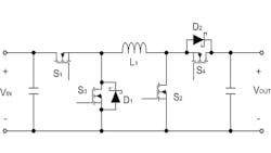
The parasitic body diode of a MOSFET usually has a higher forward voltage drop and larger reverse recovery charge than a discrete Schottky diode. Adding additional Schottky diodes in parallel with rectifier MOSFETs S3 and S4 (Fig. 3) can shunt current away from their body diodes. Therefore, the conduction loss and reverse recovery loss can be reduced and converter efficiency can be improved.
Buck-Boost Converter Design Example
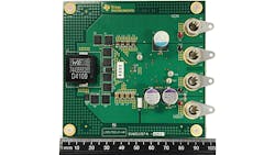
A 204W buck-boost converter evaluation module (Fig. 4) adopting LM5175 synchronous buck-boost controller has been designed, built and tested. Table 1 summarizes the key parameters of this design.
|
VIN Range (V) |
VOUT (V) |
IOUT (A) |
Output Power (W) |
Inductor (µH) |
Switching Frequency (kHz) |
|
9-36 |
12 |
17 |
204 |
2.6 |
260 |
Table 1. Key parameters of the four-switch buck-boost converter.
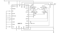
Figure 5 shows the simplified schematic, wherein two paralleling MOSFETs are used for each switch to reduce conduction loss and spread heat dissipation. Next, 60V MOSFETs are selected for Q1 through Q4 on buck leg, while 25V MOSFETs for Q5 through Q8 on boost leg. All these MOSFETs are in SON 5-mm × 6-mm package. The D1 discrete Schottky diode is added to parallel with rectifier MOSFETs of buck leg (Q3 and Q4), while D2 is added to parallel with rectifier MOSFETs of boost leg (Q5 and Q8). These two Schottky diodes are both used to shunt current away from the body diodes of rectifier MOSFETs, which helps decrease the dead-time loss and reverse recovery loss.
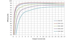
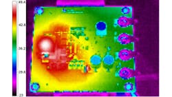
Very high efficiency has been achieved over input voltage and output current range (Fig. 6). The peak efficiency is 98.6 percent and the full load efficiency is up to 98.2 percent. Figure 7 shows the thermal image of the evaluation module at room temperature. With 9V of input voltage and 17A of output current, the hotspot, which is the inductor, of the entire board is only 49.4°C. A fairly small inductor (18.2 mm x 18.2 mm x 8.9 mm) is used in this design, and its temperature can be further reduced by using bigger inductor. The improved thermal performance eliminates the need for heat-sink for such a high-power design.
References
- “LM5175 wide VIN 4-switch buck-boost converter high power evaluation module user’s guide,” Texas Instruments, February 2015
- “AN-2178 LM5118 Four Switch Conversion,” Application Report, Texas Instruments, May 2013
- Haifeng Fan, “Design tips for an efficient non-inverting buck-boost converter,” TI Analog Application Journal (slyt584), 3Q, 2014
- Download the LM5175 datasheet
