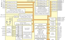
A single-chip, digital power management controller from Texas Instruments., the UCD3138064, supports many isolated power supply topologies, including: single-phase, two-phase interleaved or bridgeless power factor correction; phase-shifted full-bridge; resonant LLC; and hard-switching full-bridge. Like the other members of the UCD3138 product family the controller’s architecture employs programmable digital state machine hardware for implementing fast voltage/current loop control in conjunction with an integrated general purpose microcontroller for the necessary power supply housekeeping and system communication tasks. The controller requires external gate drivers and MOSFETs with power stage to complete a power supply design, as shown in Fig. 1.
Fig. 1.The UCD3138064 includes 64 kB of program flash memory in two 32 kB banks, enabling designers to implement one main image plus one back-up image.
This digital controller offers 64 kB of program flash memory in two 32 kB banks, allowing the storage of two firmware images. Firmware bank A can represent the space for a power supply’s current (incumbent) firmware code and bank B can represent the space for the desired updated version of the code.. You can use this arrangement when a deployed server requires a new feature or to address a possible bug or issue in the power supply. To upgrade the supply, you enter the new firmware into its designated flash memory bank. For example, a digital DC-DC supply’s existing firmware uses IOUT overcurrent protection and features no communication with its digital PFC controller on the primary side of the associated front end AC-DC power supply. Then, you can upgrade from the old firmware to a new firmware that implements constant power/constant current (CP/CC) IOUT overload protection and IPRIM (primary current) cycle-by-cycle current limiting protection while also establishing communication with the digital PFC controller. The UCD3138064 controller is capable of performing the upgrade seamlessly while continuing to keep the power supply in regulation during the firmware transition. This “on the fly update ” eliminates the need to use “hot-swap” or to physically replace a power supply due to a firmware related issue, which would interrupt system operation.
Besides the 64kB of flash memory the UCD3138064 controller contains three independent Digital Power Peripherals state machine hardware blocks, an ARM7 microcontroller core with ADCs, Timers and Communications, and other blocks for specific Power Management Functions. Each of the three Digital Power Peripherals consists of:
• High speed digital control loop with a dedicated Error Analog To Digital Converter (EADC)
• Two pole - two zero Proportional Integral Derivative (PID) digital compensator
• Digital Pulse Width Modulator (DPWM) outputs with 250ps pulse width resolution
Along with the ARM7 microcontroller, UCD3138064 offers a 12-bit, 267 ksps general purpose Analog-Digital Converter (ADC) with up to 14 channels. Timers and Communications include:
• A 24-bit, 16-bit and a watchdog timer.
• SPI high-speed synchronous serial input/output port allows a serial bit stream of programmed length to be shifted into and out of the IC at a programmed bit-transfer rate. The SPI is normally used for communication with external peripherals.
• PMBus Interface supports independent master and slave modes controlled directly by firmware through a processor bus interface. Individual control and status registers enable firmware to send or receive I2C, SMBus or PMBus messages.
• Bidirectional I2C bus consists of its serial clock and serial data lines that must connect to a positive supply through a pull-up resistor. You can initiate data transfer only when the bus is not busy.
• A maximum of two independent Serial Communication Interface (SCI) or Universal Asynchronous Receiver/Transmitter (UART) interfaces are included for asynchronous start-stop serial data communications.
Power Management functions are:
• Light load burst mode
• Synchronous rectification
• LLC and phase shifted full bridge mode switching
• Input voltage feed forward
• Copper trace current sense
• Ideal diode emulation
• Constant current constant power control
• Synchronous rectification soft on and off
• Peak current mode control
• Flux balancing
• Secondary side input voltage sensing
• High resolution current sharing
• Hardware configurable soft start with pre bias
CONTROLLER OPERATION
Topology support has been optimized for voltage mode and peak current mode controlled phase shifted full bridge and hard switched half bridge and full bridge, single and dual phase PFC, bridgeless PFC, and LLC half bridge and full bridge.
You can operate the controller in a peak current mode control configuration to maintain transformer flux balance for topologies like a phase-shifted or hard-switching full bridge converter. You can ramp an internal DAC (digital-to-analog converter) at a synchronously controlled slew rate to achieve programmable slope compensation. This eliminates the sub-harmonic oscillation and improves input voltage feed-forward
performance.
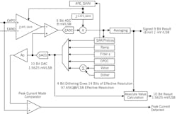
Fig. 2.Front End Module of Digital Power Peripheral contains a differential amplifier, adjustable gain error amplifier, high speed flash A/D converter, digital averaging filters, and a precision high resolution set point D/A converter reference.
A key component of the Digital Power Peripheral is its analog front end (AFE) module (Fig. 2). It comrpises a differential amplifier, adjustable gain error amplifier, high speed flash analog to digital converter (EADC), digital averaging filters, and a precision high resolution set point DAC reference. The programmable gain amplifier, EADC with adjustable digital output gain work together to provide 9 bits of range with 6 bits of resolution in the EADC output. The output of the AFE module is a 9-bit sign extended result with a gain of 1 LSB/mV. The resolution of this output is selectable to either1, 2, 4 or 8 LSBs. Other features include the ability to change the polarity of the error measurement and an absolute value mode that automatically adds the DAC value to the error.
The DPWM module implements one complete channel with two independent outputs. You can configure multiple DPWM modules to support all key power topologies. The modules can be used as independent DPWM outputs, each controlling one power supply output voltage rail. They can also be used as a synchronized DPWM, with user-selectable phase shift between the DPWM channels to control power supply outputs with multiphase or interleaved configurations.
The DPWM provides programmable dead times and cycle adjustments for current balancing between phases. It can synchronize to other DPWMs or external sources and provide synchronization information to other DPWMs or external recipients. In addition, the DPWM interfaces to several fault handling circuits.
The UCD3138064 has built in logic for optimizing the performance of its synchronous rectifier MOSFETs. This comes in two forms: synchronous rectifier MOSFET ramp, and Ideal Diode Emulation (IDE) calculation.
In discontinuous mode, the ideal on-time for the synchronous rectifier MOSFETs is a function of VIN, VOUT, and the primary side duty cycle (D). The IDE logic in the UCD3138064 takes VIN and VOUT data from the firmware and combines it with D data from the filter hardware. It uses this information to calculate the ideal on-time for the synchronous rectifier MOSFETs.
When starting up a power supply, it is not uncommon for there to already be a voltage present on the output – this is called pre-bias. It can be very difficult to calculate the ideal synchronous rectifier MOSFET on-time for this situation. If it is not calculated correctly, it may pull down the pre-bias voltage, causing the power supply to sink current. To avoid this, the synchronous rectifier MOSFETs are not turned on until after the power supply has ramped up to its nominal output voltage. The synchronous rectifier MOSFETs are then turned on slowly to avoid an output voltage glitch.
Based on an ARM 32-bit RISC (Reduced Instruction Set Computing) microcontroller (see sidebar “ARM Processor”), the UCD3138064 performs real-time monitoring, configures peripherals and manages communications. The ARM architecture includes both a 32-bit and 16-bit instruction set.
Within the UCD3138064’s architecture is a 2048x32-bit Boot ROM that contains the initial firmware startup routines for PMBUS communication and non-volatile (flash) memory download. The ARM microcontroller executes its program out of programmable flash memory as well as on chip RAM and ROM.
EVALUATION MODULES
The digital controller forms the basis for several evaluation modules. The UCD3138064EVM-166 evaluation module (EVM) is a stand-alone controller card that works seamlessly with previously released full-function power converter EVMs based on the UCD3138. For evaluating UCD3138064 operation, designers simply need to replace the UCD3138 controller card provided with these power converter EVMs with the UCD3138064EVM-166 controller card and program the appropriate UCD3138064 firmware, available upon request from Texas Instruments.
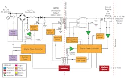
Fig. 3.Digitally controlled offline AC/DC power supply based on the UCD3138064.
The UCD3138LLCEVM-028 EVM is a digitally controlled half-bridge Resonant LLC converter. This EVM (Fig. 3) accepts DC input from 350 to 400 Vdc, and delivers a regulated 12 Vdc output rated from 0 to 340 W. Features include synchronous rectification, Constant Current/Constant Power (CC/CP) control mode, burst mode, cycle-by-cycle current limitation with duty cycle matching and current sharing to improve efficiency, system protection and overall functionality. It includes a control card pre-programmed with half-bridge resonant LLC firmware. You can program this EVM with custom firmware, allowing added functions suited to the applications needs.
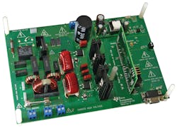
Fig. 4.The UCD3138PFCEVM-026 is a digitally controlled single phase PFC pre-regulator based on the UCD3138 (adaptable to UCD3138064).
The UCD3138PFCEVM-026 is a single phase PFC pre-regulator (Fig. 4). This EVM accepts universal ac line input from 90 to 264 Vac, 47 to 63 Hz. The nominal output voltage is 390 Vdc, Output full load power is 360 W, with over 0.999 power factor and Total Harmonic Distortion (THD) below 5% for most operating conditions. You can reconfigure this EVM to a dual-phase interleaved PFC or bridge-less PFC topologies with hardware and firmware updates.
Sidebar: ARM Processor
ARM processor architecturecovers a family of RISC computer processors designed and licensed by British company ARM Holdings. It was first developed in the 1980s by Acorn Computers Ltd. to power their desktop machines and subsequently spun off as a separate company, now ARM Holdings. Globally, as of 2013, it is one of the most widely used 32-bit instruction set architectures.
RISC is a CPU design strategy based on simplified instructions that enable faster instruction execution than complex instruction set computing (CISC). The RISC approach involves a system of small, highly-optimized set of instructions, rather than a more specialized set of instructions found in other architectures. RISC systems use load/store architecture, where memory is normally accessed only through specific instructions, rather than accessed as part of other instructions.
The ARM7TDMI-S 31.25 MHz processor is a synthesizable member of the ARM family. Its RISC architecture has two instruction sets: 32-bit ARM instruction set and the 16-bit Thumb instruction set. Thumb instructions allow higher code density that is equivalent to a 16-bit microprocessor, with the performance of the 32-bit microprocessor. The three-stage pipelined ARM processor has fetch, decode and execute stage architecture. Major blocks in the ARM processor are a 32-bit Arithmetic and Logic Unit (ALU), 32 x 8 multiplier, and a barrel shifter.
The UCD3138064 employs a Von-Neumann architecture, where a single bus provides access to all memory modules. All memory module addresses are sequentially aligned along the same address range, which applies to program flash, data flash, ROM and all other peripherals. Within the UCD3138064 architecture, a 2048 x 32-bit Boot ROM contains the initial firmware startup routines for PMBUS communication and non-volatile (flash) memory download. After power-up-reset checks to see if there is a valid flash program written it executes the boot ROM. If a valid program is present, the ROM code branches to the main flash program execution. If there is no valid program, the IC waits for a program download through the PMBus.
There are three separate flash memory areas present inside the device. There are two-32 kB program flash blocks and 1-2 kB data flash area. The 32 kB program areas are organized as 8 k x 32 bit memory blocks and are intended for firmware programs. The blocks have page erase capability for erasing blocks as small as 1 kB per page, or with a mass erase for the entire 32 kB array. The flash endurance is specified at 1000 erase/write cycles and the data retention is good for 100 years. The 2 kB data flash array is organized as a 512 x 32 bit memory (32 byte page size). The data flash is intended for firmware data value storage and data logging. Thus, the Data flash is specified as a high endurance memory of 20 k cycles with embedded error correction code (ECC). There is also a 4 kB RAM, organized as a 1k x 32 bit array, which is available for run time data storage and scratchpad memory.


