Passive circuits for power factor correction (PFC) are simple, reliable, robust, and they don't generate EMI [1-4]. Plus, they offer a low-cost alternative for complying with harmonic current limit specifications [5]. The major limitation of passive circuits has been their size and weight, which is primarily due to the associated inductor.
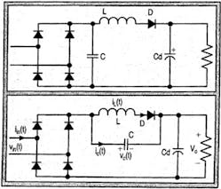
A recent investigation into reducing the size and cost of this inductor yielded an LCD circuit (referred to as LCD-1) that requires a smaller inductor than a standard solution with classical LC-filter [1-3]. With the help of an additional small capacitor and a diode, the equipment changes from Class D to Class A of IEC 1000-3-2 or EN61000-3-2 specifications. The advantage of having equipment in Class A is that its limits are absolute, allowing more distortion at low power levels up to 300W. Fig. 1(a) shows the LCD-1 PFC circuit.
Figure 1. Circuit diagram of LCD circuits: LCD-1, top; LCD-2, bottom.
LCD-1 simulations assumed the output filter capacitor is large, so output voltage ripple is negligible [3]. However, most of the passive PFC circuits have 5% to 20% ripple in their output. The switchmode dc-dc converter stage that follows has sufficiently large bandwidth to reduce line frequency ripple in its output. Guidelines for the LCD-1 design don't give the minimum value required to achieve compliance, which is important for comparison with other similar circuits [3].
To determine the minimum inductance required for compliance, we simulated the effect of ripple voltage on the LCD-1 circuit's behavior. LCD-1 performance changes with output ripple, so the minimum inductance required for the compliance increases with a ripple increase. These limitations are absent in the updated LCD-2 circuit presented in Fig. 1(b). This circuit is relatively insensitive to ripple, and the size of the inductance required for compliance is substantially less than that required in LCD-1, thereby reducing cost. Extensive simulations of 100W circuits and comparative experiments demonstrated the advantage and benefits of LCD-2.
Output Voltage Ripple
Exact mathematical analysis of the LCD-1 circuit is possible but intricate; it's adequate to repeatedly simulate the circuit for understanding its principles [3]. We can evaluate the circuit by using an example of a 230V, 50 Hz input and 1 kΩ load resistance for about a 100W output. Altering the value of Cd changes the output voltage ripple.
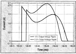
Figure 2. Simulated input current waveform of LCD-1 for half-line period for 10% and 2.5% output voltage ripple.
Fig. 2, on page 30, shows simulated input current waveform for a half-line period for 10% and 2.5% output ripple voltage. The component values used for the simulation are: L = 5.5 mH, C = 45 μF and Cd = 300 μF (for 2.5% ripple) and 75 μF (for 10% ripple). The values of L and C used in the simulation are randomly selected to see the general effect of output voltage ripple on the input current waveform. The input current pulse width shortens with the increase in output ripple. This means the following:
-
If the values of L and C are optimized to classify the waveform as Class A for a particular output ripple, then increasing output ripple may change the equipment back to Class D.
-
Peak input current and total harmonic distortion (THD) increases and the overall power factor decreases with increasing output ripple.
-
Higher ripple voltage demands higher inductance to classify and comply with IEC 1000-3-2 Class A limits.
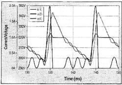
Normally, in LCD circuits the voltage across C is less than the output voltage, and diode D prevents the resonant “recharge” of the capacitor C through L and Cd[3]. However, reducing Cd to allow higher output ripple may cause the instantaneous output voltage to become less than the voltage across C. This will form a local resonant circuit of L, C, and Cd as diode D doesn't prevent the “discharge” of C. These oscillations occur when all the diodes of the bridge rectifier are off and therefore don't reflect on the line current. However, the local resonant circuit increases rms current ratings of L and C and reduces efficiency. Making Cd 33 μF produces local oscillations due to the discharge of C (Fig. 3).
Figure 3. Oscillatory inductor current [i(l1)] in LCD-1 due to discharge of C; v(3) and v(4) are bridge and output voltage, respectively.
LCD-2
The LCD-2 circuit of Fig. 1(b), on page 28, is a topological variation of LCD-1. Both the circuits behave identically under the zero output ripple assumption. However, the presence of ripple alters their operation.
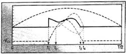
Figure 4. Waveforms of LCD-2 in steady-state for one half of line period. [___: iin(t), ...:iC(t)-.-:iL(t)-..-:vC(t) and ---:vin(t)]
Fig. 4 shows some of the important characteristic steady-state waveforms of the circuit for one half-line period. There are four distinct sub-intervals of operation. For the interval 0 ≤t≤t1, the instantaneous line voltage is less than Vo - VCL (C charges to - VCL in the previous cycle of operation). The diodes of the bridge rectifier therefore don't conduct. At t = t1, the instantaneous line voltage reaches Vo - VCL and current iC(t) starts flowing from the input through C and Cd. The initial step in iC(t) depends on the instantaneous line voltage and the capacitive reactance of the path. During t1 ≤t≤t2, iC(t) discharges C and at t = t2, vC(t) becomes zero. Diode D now starts conducting and the current iL(t) flows through the inductor L. After t = t2, the input current iin(t) is the sum of iC(t) and iL(t). This continues till t = t3 when iL(t) = -iC(t). The bridge rectifier diodes stop conducting. In the next time interval t3 ≤t≤t4, L and C oscillate through diode D. This mode ends when iC(t) and iL(t) drop to zero and C charges to - VCL. For the remaining period of the half cycle (t4 ≤t≤T/2), there's no current in the circuit except for the filter capacitor Cd feeding the load.
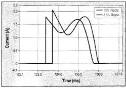
Figure 5. Simulated input current waveform of LCD-2 for half-line period for 10% and 2.5% output voltage ripple
Simulations for LCD-2 also involved a 230V, 50 Hz input for 100W output and two values of output voltage ripple. Fig. 5 shows its input current waveform over half-line period with 2.5% and 10% output ripple voltage. The component values used for the simulation are: L = 2 mH, C = 60 μF and Cd = 300 μF (for 2.5% ripple) and 75 μF (for 10% ripple). The output ripple has no significant effect on the input current pulse width, although there's a marginal increase in pulse width and decrease in the peak current with the increase in the output ripple. This effect is opposite to the one observed in LCD-1.
Compliance Characteristics
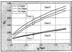
Figure 6. Range of normalized L/C values for which input current of LCD-2 is classified as Class A.
Simulations show, even for LCD-2, a range of inductance and capacitance values for which you can classify the input current as Class A. Fig. 6 shows this range in the normalized form for different percentages of output ripple. The inductance and capacitance values are normalized (LN and CN, respectively) with respect to the base values:
Where:
f = Line frequency
Vin = rms line voltage
Po = Output power
However, changing the input current from Class D to Class A doesn't automatically guarantee compliance. For a given value of L, as the value of C (in the limiting region of Fig. 6 for Class A) increases the peak input current, the harmonic content also increases. Therefore, you should use the lowest value of C required to just classify the current waveform as Class A for given value of L. The harmonic limits specified in IEC 1000-3-2 Class A norms determine the minimum value of L for a given output power. At low output power, the Class A limits are many times higher than the actual harmonic content. Therefore, the value required to classify the waveform as Class A determines the minimum inductance. Because of the higher initial input current step, at higher output power the higher order harmonics may exceed the limits. Keeping these harmonics within the limits requires a larger inductance than minimum required for Class A waveform.
In the LCD-2 circuit diode, D is forward biased only when the bridge diodes are conducting and for the rest of the half-line period it's reverse biased. Therefore, unlike LCD-1, the local oscillations don't occur in LCD-2, which eliminates circulating currents.
Compliance Inductance
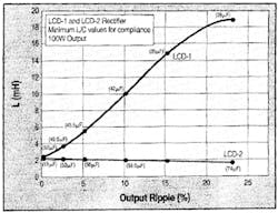
Figure 7. Minimum L/C values required for compliance for LCD-1 and LCD-2.
We performed simulations to find the minimum values of L and C for compliance of 100W LCD-1 and LCD-2 circuits for different output ripple. Fig. 7 shows that, for LCD-1 the required inductance increases sharply from 2.3 mH for 0.25% output ripple to 9.9 mH for 10% output ripple. For LCD-2, required inductance reduces from 2.2 mH for 0.25% output ripple to 2 Mh for 10% output ripple. This is consistent with the earlier observation that the input current pulse widens marginally with the increase in output ripple. For both the curves, the values in the parenthesis are the corresponding minimum values for C.
The physical size of the inductor depends on its area product, which is proportional to the inductance value, peak current, and the rms current. Area product also depends on other factors like ripple frequency, allowable core losses, window filling factor and current density, which are fixed for specified material, application, and specifications. You can use the area product coefficient K as an index of the actual inductor size:
Where:
Irms = rms inductor current
Ipk = Peak inductor current
Simulating LCD-1 and LCD-2 with the minimum values of L/C given in Fig. 7 yields the peak and rms inductor current shown in Fig. 8(a). In LCD-1, peak and rms inductor current reduce with the increase in the ripple voltage because of the higher inductance required for compliance at higher output ripple.
Figure 8. LCD-1 and LCD-2 inductor comparison with 100W output: Peak and rms inductor current with corresponding minimum L C values, left; Inductor size index K for different ouput ripple, right.
In LCD-2, however, the peak and rms current increases with the output ripple because of the lower inductance required. In LCD-1, the increase in the inductance initially dominates the size of the inductor over the reduction of peak and rms current with output ripple. Therefore, the size of the inductor also increases with the ripple as indicated by size index K in Fig. 8(b). In LCD-2, the size of inductor reduces progressively with increasing ripple. However, this reduction isn't very significant and the practical size of the inductor might be the same for different output ripple. LCD-2 requires a smaller inductance for practical values of the output ripple voltage.
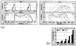
Fig. 9(a), on page 34, shows the input and inductor current waveforms for 100W LCD-1 and LCD-2 circuits with respective minimum L/C values and for output voltage ripple of about 0%, 2.5%, 5%, 10% and 20%, respectively in the direction of the arrow. The input current of LCD-1 is almost centered in the half-cycle of the sine wave — except for the case of 20% output ripple. There, local oscillations due to discharge of C cause the input current pulse to shift away from the center. This makes the displacement power factor (DPF) very high.
Figure 9a. Input and inductor current waveforms of two circuits (LCD-1, left; and LCD-2, right) for 100W output.
Figure 9b. Displacement angle for different output ripple.
In LCD-2, the input current pulse shifts progressively away from the center with increasing ripple, and DPF degrades accordingly. The displacement angle of both the circuits are in Fig. 9(b). Therefore, if the two circuits have similar input currents, the overall power factor of LCD-1 is better than that of LCD-2.
In LCD-1, L, C, and Cd suppress high-frequency noise or spikes generated by the load before propagating to the source and vice versa. However, in LCD-2 the load and source are capacitively coupled, therefore the circuit offers no attenuation.
The voltage across C in LCD-2 is bipolar (Fig. 4, on page 30) and very low in steady state, compared with the peak line voltage. During transients (start-up or load short-circuit) high voltage will appear across C. Therefore, C should be an ac capacitor that you can emulate using two electrolytic capacitors connected back-to-back with anti-parallel diodes. However, C is always subjected to rectified peak line voltage in LCD-1.
Verification
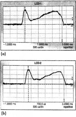
To verify the input current experimentally, we built a test circuit for LCD-1 and LCD-2. For both the circuits, Vin = 230V, 50 Hz from a line of unknown impedance, Cd = 141 μF (three paralleled 47 μF) for about 5% output voltage ripple and the load resistance was 1 kΩ. The values of L/C were 5.5 mH/35 μF for LCD-1 and 2.5 mH/50 μF for LCD-2.
Figure 10a. Experimental input current: LCD-1.
Figure 10b. Experimental input current: LCD-2.
Figs. 10(a) and (b) show the experimental input current waveforms of both the circuits, which are almost identical to each other. The peak voltage across C is 324V in LCD-1 and 19V in LCD-2. The overall size of this capacitor assembly is much smaller than the single high-voltage electrolytic capacitor required in LCD-1. External core volume of the 2.5 mH inductor used in LCD-2 is 1.64 × 10⁻⁵ m3, compared with 3.27 × 10⁻⁵ m3 for the 5.5 mH inductor used in LCD-1.
References
-
M.M. Jovanovic and D.E. Crow, “Merits and Limitations of Full Bridge Rectifier with LC Filter in Meeting IEC 1000-3-2 Harmonic Limit Specifications,” APEC 1996, pp. 354-360.
-
R. Redl and L. Balogh, “Power Factor Correction in Bridge and Voltage Doubler Rectifier Circuits with Inductors and Capacitors,” APEC 1995, pp. 466-472.
-
R. Redl, “An Economical Single-Phase Passive Power Factor Corrector Rectifier: Topology, Operation, Extensions and Design for Compliance,” APEC 1998, pp. 454-472.
-
Nathan O. Sokal, K. Kit Sum, David C. Hamill, “A Capacitor-Fed, Voltage-Step-Down, Non-Isolated Rectifier,” APEC 1998, pp. 208-215.
-
“Electromagnetic Compatibility (EMC) — Part 3: Limits — section 2: Limits for Harmonic Current Emission (equipment input current ≤ 16A per phase),” IEC 1000-3-2 Document, First Edition, 1995.
For more information on this article, CIRCLE 332 on Reader Service Card
