Members can download this article in PDF format.
With rapid adoption of electric vehicles and bulk installation of solar photovoltaic power systems, electric-vehicle (EV) charging—especially fast charging—and solar power availability pose a challenge for the utility grid. Overall, the grid lacks the capacity to deliver high power and store surplus solar electricity.
In particular, the increasing connection of alternative-energy sources to the low- or medium-voltage grid requires accelerated development of power-efficient, reliable energy systems and integration with grid-connected resources such as energy-storage systems and EV charging infrastructure. For example, many residences now use a combined solar-energy generation and battery energy-storage system to make energy available when solar power isn’t sufficient to support demand.
Power-Stage Topologies
Let’s begin by examining topology considerations for designing power stages commonly used in solar inverters and energy-storage systems (ESS).
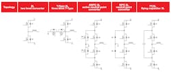
Three-level topologies are the most widely used in solar applications (Fig. 1). Such topologies allow for the use of smaller passive components and have lower electromagnetic interference (EMI) compared to two-level converters. They have clear advantages in terms of power density, reliable operation, and fast time-to-market over traditional two-level converters.
The first converter we’ll look at is the T-Type three-level converter. The name T-Type is derived from the way the transistors are arranged around the neutral point, VN (Fig. 1, Q1 and Q2), and connect between the dc link; Q3 and Q4 are in series with VN. Since Q3 and Q4 connect to VN, they only see half of the bus voltage—they can be rated at 600 V in an 800-V dc-link voltage system, which saves cost with this converter type.
Next is the active-neutral-point-clamped three-level converter (ANPC 3L). In the example in Figure 1, the VN is connected with active switches. VN connects through diodes D5 and D6 and sets VN in the middle between the dc-link voltage. When turning off this converter, it’s important to limit all voltages across each switch to half of the dc-link voltage. The control microcontroller (MCU) must handle the shutdown sequencing.
Neutral-point-clamped (NPC 3L) inverters (Fig. 1, again) comprise a family of multilevel power converters that are characterized by the use of clamping diodes to guarantee the proper voltage sharing across the power switches. In this case, the VN is connected via diodes. It sets the neutral point at the middle between the dc-link voltage.
The NPC topology’s slightly lower cost compared to the ANPC topology comes at the expense of slightly lower efficiency. The requirements for shutdown sequencing also are identical to the ANPC topology.
At this point, you may well be thinking “What is the difference between NPC and ANPC?” Simply put, under the same switching frequency, the ANPC converter has a lower current total harmonic distortion (THD) compared to the NPC converter, while the losses are higher.
The last topology in the group is the flying capacitor three-level converter (FC 3L). In the flying capacitor topology, the additional voltage levels are synthesized by high-frequency (so-called) flying capacitors. The voltage across the capacitor is limited to half the dc-link voltage and shifts periodically between V+/V−.
In ANPC, NPC, and flying cap, all switches can be rated half of the dc-link voltage. That saves cost, but all three require shutdown sequencing, which must be handled by the controller MCU.
Empowering a More Sustainable Future
As power requirements increase, voltages also must ramp up to minimize losses through heat. For example, EVs, which run on 400- or 800-V battery packs, use high-voltage designs that improve charge times and extend driving range, helping eliminate barriers to EV adoption.
A traction inverter manages the flow of energy from the high-voltage battery pack to the motor, turning the wheels and propelling the vehicle. One of the most significant changes pushing EV performance is a transition from insulated-gate bipolar transistors (IGBT) to silicon-carbide (SiC) technology for the high-voltage switches used in a traction inverter.
Because SiC transistors are more efficient—turning more stored battery input into usable motor output—than IGBTs, they’re a natural upgrade. Furthermore, SiC transistors are smaller than IGBTs and run cooler, further reducing weight, siz,e and energy waste in the drive system.
Designing Bidirectional EV Charging Systems
When an EV is charged, ac from the grid is converted to dc so that it can be used by a car (Fig. 2). With traditional one-way EV chargers, electricity flows from the electric grid into the electric vehicle. With two-way (bidirectional) EV chargers, electricity can flow both ways, supporting vehicle-to-grid or vehicle-to-home use cases.
The power stage works as a battery charger in one direction. In the other direction, it becomes a constant voltage dc-dc converter to convert the variable battery voltage to the required constant bus voltage level.
Pinpointing the Right Solution
Solar energy plays an important role in renewable-energy generation since it’s clean, pollution-free sustainable energy. TI products enable efficient power delivery and a smarter grid that meets global compliance standards and supports future load patterns for long-term reliability.
Advances in the field of power electronics in tandem with semiconductor technology offer everything you need to meet topology considerations for designing power stages commonly used in solar inverters and ESS.


