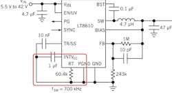
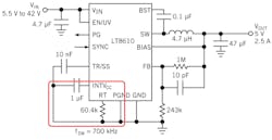
The hot loop with the main switching energy is the major source of RF energy. However for the operation of the IC and circuit, other AC carrying loops are required. All circuits need a supply for the main switch driver. In the case of the buck, it is often decoupled with the same VIN capacitor as the hot loop. Other ICs use a separate voltage for the drive circuit, often referred to as INTVCC(Fig. 14).
Make the INTVcc capacitor PGND and GND loop as small as possible and shield it with a solid plane in the next layer. EMI energy is on the order of 20dB lower than in the main hot loop. Any excessive inductance in the INTVcc loop will deteriorate IC performance. The INTVcc capacitor decouples beside switch drive internal sensitive and wide band circuitry like current sense comparators, reference and error amplifiers which are very often internally supplied from INTVcc too.
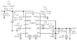
The LT8610 LTspice® circuit (Fig. 15) uses L2 with a high loss of RPAR = 1Ω to decouple the zero impedance LTspice voltage source, V1, from the input capacitor, C6. Note: LTspice switch mode regulator models are developed to simulate the functionality of the IC. Use great caution to extrapolate RF behavior because the models do not account for the internal or the external lump devices or board layout. However, it is nonetheless a great tool to get an approximation of very difficult to measure effects.
External Switch Drive Signals
After the main hot loop and the INTVccdecoupling loop, the next EMI trouble sources are often external switch drive signals. Even modern MOSFETs have single-to-dual digit nanofarad effective input capacitance. Their drivers often have drive currents in the single amp range, with rise and fall times approaching single digit nanoseconds.
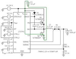
The green loop (Fig. 16) shows the current path for the bottom gate current. It is supplied from the C1. Make sure that the loop is small. The Q2-source GND to C1 GND connection is most easily accomplished with a solid GND area in the next layer under the component layer.
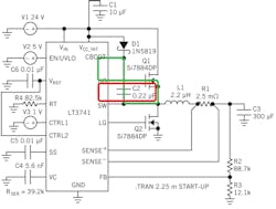
The red and green loop (Fig. 17) shows the top gate drive current loops. They are supplied from the boost capacitor, C2, and the return is the SW connection to the controller IC. Keep the red loop small and place the traces parallel with only a small gap. If C2 is placed close to the controller IC, the green loop will also become small.
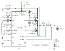
The green loop (Fig. 18) shows the recharge of the boost capacitor. If you have already made the above loops small and have placed D1 relatively close, this loop is also small.
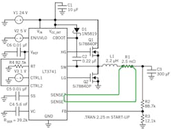
The sense amplifier in Fig. 19 checks the SENSE+ and SENSE– on the small shunt voltage over R1 to terminate the top switch on cycle. Even sub-millivolt noise will result in duty cycle jitter. Coupling to any of the former transmitting loops should be minimal. First, this loop area needs to be small as well, so make the gap between the SENSE+ and SENSE– line minimal. Then place the loop traces on the other side of a shielding plane from the high current loops mentioned above. If enough layers are available, the SENSE+ and SENSE– line can be on top of each other if there are not significant magnetic AC fields parallel to the PC board layers. If SENSE+ and SENSE– filtering is used, place the filter close to the controller IC, since R1 is always low impedance and the sense inputs are higher impedance.
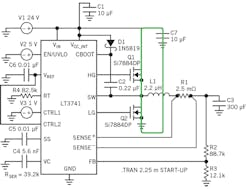
The main hot loop in Fig. 20 consists of the external MOSFETs Q1 and Q2 and the closest low impedance decoupling capacitor C7. This is the loop with the highest RF energy in a controller solution.
How Shielding Works
DC magnetic fields go through air, FR4 epoxy dielectric and copper almost undisturbed. AC magnetic fields are impacted only by the induced currents in a conductor—usually copper or tin, etc. So, absent from ferromagnetic material, we can focus on currents as the only source to alter or attenuate AC magnetic fields in a typical PC board environment.
We know from experiments that complete conductive enclosures have a very high attenuation—easily over 100dB—over a very broad frequency range above the AM band. Cookie boxes are a popular example widely used in the R&D community to shield sensitive circuitry, to enable high frequency (HF) measurements. For HF circuits you can buy them in rectangular form which fits easier for PC boards and HF connectors like BNC, N, SMA, etc. For practical purposes HF magnetic fields do not escape closed conductive boxes as long as the wall is thicker than skin depth.
How Effective is a Shield?
If the board copper plane were non-conductive, it would be transparent to any magnetic field like a sheet of paper. The current in the copper is the only source of influence on the magnetic field. The energy available for eddy currents is induced in the shield. Such currents will cancel any magnetic field inside the copper shield and outside in the direction away from the inducing current, within the limits of skin and proximity effect.
The cancellation layer is the layer that cancels the magnetic field from the inducing currents (i.e., from the hot loop) and induced currents in the shield. So it is sort of midway between the AC currents in opposite directions. The position of the cancellation layer can be estimated by rule of thumb and may help you visualize how the remaining AC fields look.
The closer the cancellation layer is to the induced current layer, the better the cancellation. Inductance is the integral of the magnetic field—the same magnetic field that forms the near field RF antenna. All of these effects are reduced when the cancellation layer is placed closer to the inducing current loop.
What Works Even Better?
If the current returns through the plane, the situation is somewhat different. Now the current in the plane is not only passive induced, but is the active return flow.
It is forced to be same as the current in the top trace. The benefit is that the cancellation is now closer to the inducing trace, in this case halfway between the top layer current and the returning current in the plane. Because the cancellation layer is now half the distance to the inducing current, it is safe to say that the magnetic field is now lower by at least a factor of two compared to the above situation with passive shielding only.
If you can, lay out the board to let the return current flow in the closest layer. Make its dielectric (isolation) as thin as practical. It is better to have the return current flow in the closest trace to the inducting current with minimum dielectric distance. That’s what solid GND planes do by default.
Standard multilayer boards often have much thinner outer layer dielectrics to help reduce EMI.
Line Conducted EMI Measurements
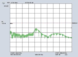
Fig. 21 shows an LT8611 IC with some input filtering with a ferrite bead and 4.7µF ceramics line conducted from 30MHz to 400MHz. The display line of –67dBm corresponds to 40dBuV.
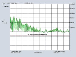
Fig. 22 shows an LT8610 power supply 13V in, 5V out at 1A out, line conducted up to 900MHz. In Fig. 22, an additional wideband amplifier (LNA) in the HF signal chain with 35dB gain is used. So the –100dBm spectrum analyzer display line corresponds to –135dBm, which is the thermal noise floor of a 50Ω system with 10kHz bandwidth at room temperature. The main HF energy needed to be filtered out of the LT8610/LT8611 is below 400MHz. +10dBuV corresponds to 3.16 µVRMS.
EMI Optimization
Designers should follow these methods to optimize EMI characteristics in the PC board. First, check the layer stack. Use a PC board of four layers or more if possible. The second layer from top is typically only about 200µm distance, and a shield will cancel the hot loop much better than any shield over 1mm away in a dual layer board.
In the hot loop shield, the same current as in the top trace hot loop runs as eddy current. Keep the layer two shield solid. Place vias away from the hot loop for connections to GND planes you want to keep quiet. The hot loop shield cancellation currents create HF voltage across the loop, and you do not want to couple it with vias in areas you need quiet. This current decays with distance, but often remains a problem.
The challenge for filtering the input and, if required, the output is mainly in finding an area that is quiet enough. An effective way is to make a complete GND ring around the the power supply unit (PSU) connected with vias.
Filter capacitor GND return should be at the location where the VIN current crosses the ring. There should be still filtering inductance in the direction of the hot loop. This inducstance could be present in a ferrite bead or an inductor.
Magnetic Coupling
Another consideration for design engineers is to beware of magnetic coupling between filter inductors and the main inductor. The transformer action can jeopardize your attenuation. Place filter inductors at a distance from the main inductor.
Use short ceramic capacitors, i.e., 0402, or reverse geometry capacitors. Keep in mind that block capacitors need low equivalent series inductance (ESL) which mainly dictates their impedance. Shorter and thicker capacitors have lower ESL.
Characteristic impedance of the strip lines you create with your VIN traces is in the low single digit Ohm area. The ESL of your block capacitors should be as low as possible. Use reverse geometry capacitors or a stack of 0402 closest to the filter point and larger cases close by. Any trace length significantly increases the few hundred pH inductance your small block capacitors have.
Finally, ensure that the routing path of the VIN and the return trace goes through the filter capacitor pads. This avoids additional performance-degrading trace inductance.
